| Posted: Aug 21, 2008 | |
Focusing on nanotechnology - pushing the limits of X-ray microscopy |
|
| (Nanowerk Spotlight) X-rays are at the short wavelength, high energy end of the electromagnetic spectrum (only gamma rays have shorter wavelength and carry more energy) and this form of radiation is primarily used for crystallography and diagnostic radiography. Due to the high energy they carry, and because their wavelengths are on the order of the size of atoms, X-rays can penetrate deeply into a material. Chances are you've had an 'X-ray' taken at least once in your life by your doctor or dentist but you will have also encountered X-ray machines at airport security (the machines your carry-on luggage is going through). X-rays play an important role in microscopy and X-ray microscopes have become very powerful scientific instruments for domains such as nanotechnology, materials and life sciences, microelectronics, and chemistry. | |
| Depending on the level of energy they carry, X-rays are termed 'hard' – highest energy rays, typically between 8-100 thousand electron volts (keV) – or 'soft' – lower energy rays from roughly 1-8 keV – however this distinction is not well defined. By combining the magnifying power of optical microscopy with the penetrating power of X-rays, X-ray microscopes can generate highly detailed two-dimensional images of features down into the nanoscale, including their internal structure and quantitative chemical information. | |
| The reliable and efficient focusing of hard X-ray beams to nanoscale dimensions is an important – and very challenging – prerequisite for many experimental techniques. A common device used for this is a so-called Fresnel zone plate (FZP). | |
| FZPs have proven to give focal spots with excellent spatial resolution combined with low background. In the soft X-ray range, FZPs can reach a resolution below 20 nm but so far this high-resolution potential could not be exploited with hard, high-energy X-rays. The fabrication of devices to focus hard X-rays is one of the most difficult—and important—challenges in nanotechnology. | |
 |
|
| Fresnel zone plate (Image: Georg Wiora) | |
| "The nanofabrication of hard X-ray Fresnel zone plates is a very difficult task because of extreme and conflicting technical requirements" Dr. Yong Chu explains to Nanowerk. "Spatial resolution requires very thin outermost zones. However, high efficiency with weakly absorbed hard X-rays imposes a high aspect ratio. The reconciliation of such requirements is problematic: stable thin nanostructures with high aspect ratio are difficult to fabricate. As a result, progress was so far limited to soft X-rays and the spatial resolution for hard X-rays remained above 40–50 nm. This is regrettable since it rules out many important applications in biomedical research, most notably subcellular structure studies in tissues." | |
| Chu, a senior scientist at Argonne National Laboratory, is a member of an international collaboration involving the U.S., Switzerland, Taiwan and South Korea that has now been able to demonstrate that Fresnel zone plates combining 30 nm external zones and a high aspect ratio finally bring hard X-ray microscopy beyond the 30 nm Rayleigh spatial resolution level and measurable spatial frequencies down to 20–23 nm feature size. | |
| The scientists published their findings in the August 8, 2008 online edition of Nanotechnology Full-field hard X-ray microscopy below 30 nm: a challenging nanofabrication achievement. | |
| "Our focusing device pushes the record of spatial resolution in radiology to a new level that is particularly important for studies of cells," says Dr. Yeukuang Hwu, a collaboration member and senior scientist at the Academia Sinica in Taiwan. | |
 |
|
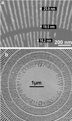
| (a) SEM micrograph of a resolution pattern fabricated at Academia Sinica, showing the central area with the smallest lines of width <20 nm. (b) X-ray micrograph of the same pattern demonstrating the visibility of features smaller than 20 nm. (Reprinted with permission from IOP Publishing) | |
| He explains that he and his partners made the circles of the FZP out of lines of gold over a 1 µm thick silicon nitride membrane. "The difference with respect to visible-light zone plates is that the circles are very small and thin, in the range of tens of nanometers" he says. "Their fabrication is very complicated since to interact with X-rays – that are weakly absorbed – the lines must also be quite deep. Our approach solved the problem of combining small thickness and large depth, pushing the X-ray lens focusing performance to new limits." | |
| The researchers attribute their achievement to several factors: 1) Two empirical optimization procedures – a difficult but apparently critical step – for the e-beam dose and for the pattern duty cycle. 2) The high (100 keV) electron energy for e-beam writing and the use of current pulses for gold electrochemical deposition. | |
| "The high electron energy enabled us to focus the electron beam down to a 5 nm diameter and reduce backscattering related problems" Hwu points out. "As to pulsed electrodeposition, the optimized parameters for our best FZPs were a 0.2 second pulse width, a 40 second pulse distance, room temperature and a current density of 0.5 ASD (ampere per square decimeter). Pulsed electrodeposition was specifically better than DC electrodeposition in filling the narrow trenches of the outermost FZP zones." | |
| The optimized nanofabrication procedure enabled the scientists to achieve the required FZP characteristics not only for resolution but also for efficiency. "The resolution only depends on the outermost zone width whereas the efficiency depends on the metal structure thickness" explains Dr. Giorgio Margaritondo, a collaboration partner from Switzerland and professor at the Ecole Polytechnqiue Fédérale de Lausanne. "The efficiency is important not only for time-resolved applications but also to reduce negative effects, for example, of vibrations and background inhomogeneities – a limited photon flux leads to long exposure times that worsen such effects." | |
| The potential impact of this work touches many different areas: materials science, microelectronics, nanophotonics, the life sciences and other domains. Margaritondo says that the demonstration that features of less than 20 nm are easily visible opens the door, for example, to microradiology of subcellular details in thick tissue specimens, of deep DRAM features, of inside nanofeatures in fuel cells and of many other fundamental and/or technological objects. | |
| He also notes that the nanofabrication procedures used by the team have not yet reached their natural limits, so they are pushing towards even thinner and deeper gold lines in the pursuit of new spatial resolution records for nanoradiology. | |
 By
Michael
Berger
– Michael is author of three books by the Royal Society of Chemistry:
Nano-Society: Pushing the Boundaries of Technology,
Nanotechnology: The Future is Tiny, and
Nanoengineering: The Skills and Tools Making Technology Invisible
Copyright ©
Nanowerk LLC
By
Michael
Berger
– Michael is author of three books by the Royal Society of Chemistry:
Nano-Society: Pushing the Boundaries of Technology,
Nanotechnology: The Future is Tiny, and
Nanoengineering: The Skills and Tools Making Technology Invisible
Copyright ©
Nanowerk LLC
|
|
|
Become a Spotlight guest author! Join our large and growing group of guest contributors. Have you just published a scientific paper or have other exciting developments to share with the nanotechnology community? Here is how to publish on nanowerk.com. |
|