| Posted: Aug 07, 2006 | |
Towards molecular electronics |
|
| (Nanowerk Spotlight) A potential solution to overcoming the fundamental scaling limits of silicon-based electronic circuitry is the use of a single molecular layer that self-organizes between two electrodes: so-called molecular electronics. Nature itself is highly efficient in using self-organized structures for electronic transport (photosynthesis in plants, nerve cells, etc.), and now similar self-organization of organic molecules is used to make electronic devices. Electric transport through single molecules has been studied extensively by both academic and industrial research groups. It has been demonstrated that the size of a diode, an element used in electronic circuitry, can be reduced reproducibly below 1.5 nm. Transport data, however, typically differ by many orders of magnitude and the fabrication hurdle is reliability and yield. Researchers in The Netherlands now have demonstrated a technology to manufacture reproducible molecular diodes with high yields (>95 %) with unprecedented lateral dimensions of 100 µm. | |
| For technological applications, molecular tunnel junctions must be reliable, stable and reproducible. Self-assembled monolayers (SAMs) may offer a promising route to the fabrication of reliable devices, and charge transport through SAMs of alkanethiols within nanopores is well understood, with non-resonant tunneling dominating the transport mechanism. Unfortunately, electrical shorts in SAMs are often formed upon vapor deposition of the top electrode, which limits the diameter of the nanopore diodes to about 45 nm. | |
| Dr. Bert de Boer, Assistant Professor, Molecular Electronics Group at the Materials Science Centre at the University of Groningen in the Netherlands, explained his center's current research to Nanowerk: "We have demonstrated the fabrication of molecular metal-insulator-metal (MIM) junctions with unprecedented device dimensions and obtain reproducible results with a high yield of working devices (almost unity). This low-cost technology for the facile and highly reproducible fabrication of large-area molecular MIM diodes is the first technique that allows academic groups to investigate charge transport through molecules with conventional processing techniques and can be used to realize crossbar arrays." | |
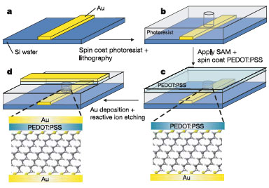 |
Processing steps of a large-area molecular junction. a, Gold electrodes are vapor-deposited on a silicon wafer and a photoresist is spin-coated. b, Holes are photolithographically defined in the photoresist. c, An alkane dithiol SAM is sandwiched between a gold bottom electrode and the highly conductive polymer PEDOT:PSS as a top electrode. d, The junction is completed by vapor of gold through a shadow mask, which acts as a self-aligned etching mask during reactive ion etching of the PEDOT:PSS. The dimensions for these large-area molecular diodes range from 10 to 100 µm in diameter. (reprinted with permission from Nature Publishing Group) |
| De Boer states that for industry, compatibility and integration of molecular electronics with CMOS technology is within reach due to the facile replacement of gold by copper and utilization of the standard process flow charts. "We demonstrate a technology that can be integrated into electronic circuits and will pave the way for molecular electronics." | |
| Key ingredients of the molecular diodes fabricated by the Dutch scientists are the use of a conducting polymer barrier in between the SAM and the metal top electrode, which prevents the penetration of vapor-deposited gold atoms into the monolayer, and processing of the diodes in via holes of lithographically patterned photoresist. | |
| "The conducting polymer acts as a cushion for the metal atoms to land on and prevent the metal atoms from penetration into the molecular layer, forming electrical shorts" says de Boer. "Furthermore, the processing of the diodes in via holes of lithographically patterned photoresist prevents the exposure of the junctions to air (oxygen/water) and makes them stable for at least 75 days." This technology can be scaled up to large areas. | |
| A recent paper about this work, titled "Towards molecular electronics with large-area molecular junctions" was published in the May 4, 2006 edition of Nature. | |
 By
Michael
Berger
– Michael is author of three books by the Royal Society of Chemistry:
Nano-Society: Pushing the Boundaries of Technology,
Nanotechnology: The Future is Tiny, and
Nanoengineering: The Skills and Tools Making Technology Invisible
Copyright ©
Nanowerk LLC
By
Michael
Berger
– Michael is author of three books by the Royal Society of Chemistry:
Nano-Society: Pushing the Boundaries of Technology,
Nanotechnology: The Future is Tiny, and
Nanoengineering: The Skills and Tools Making Technology Invisible
Copyright ©
Nanowerk LLC
|
|
Become a Spotlight guest author! Join our large and growing group of guest contributors. Have you just published a scientific paper or have other exciting developments to share with the nanotechnology community? Here is how to publish on nanowerk.com.