| Posted: Oct 22, 2008 | |
Nanotechnology - not that green? |
|
| (Nanowerk Spotlight) There is a general perception that nanotechnologies will have a significant impact on developing 'green' and 'clean' technologies with considerable environmental benefits. Just take a look at the 30+ Spotlights we have written about the use of nanotechnology in areas ranging from water treatment to energy breakthroughs and hydrogen applications. As a matter of fact, renewable energy applications probably are the areas where nanotechnology will make its first large-scale commercial breakthroughs (see: Nanotechnology applications could provide the required energy breakthroughs). | |
| Conflicting with this positive message is the growing body of research that raises questions about the potentially negative effects of engineered nanoparticles on human health and the environment (again, we have plenty of articles on this risk topic in our Spotlight series. | |
| However, there is one area of nanotechnology that so far hasn't received the necessary attention: the actual processes of manufacturing nanomaterials and the environmental footprint they create, in absolute terms and in comparison with existing industrial manufacturing processes. Analogous to other industrial manufacturing processes, nanoproducts must proceed through various manufacturing stages to produce a material or device with nanoscale dimensions. | |
| A recent overview article in the Journal of Industrial Ecology explores manufacturing routes of nanoproducts, with special attention focused on attributes likely to have significant environmental implications ("Toward Sustainable Nanoproducts"). The article was written by three scientists at the University of Illinois at Chicago (UIC) – first author Hatice Sengül,Siddhartha Ghosh, and Thomas Theis. | |
| Apart from certain nanoparticles and carbon nanotubes, the volume of mass produced nanomaterials is relatively modest, especially when compared with the total output of chemicals. Nevertheless, a number of the materials used in nanoproducts are rare, with demand sometimes exceeding production (see for instance: "Ultrathin transparent graphene films as alternative to metal oxide electrodes"). | |
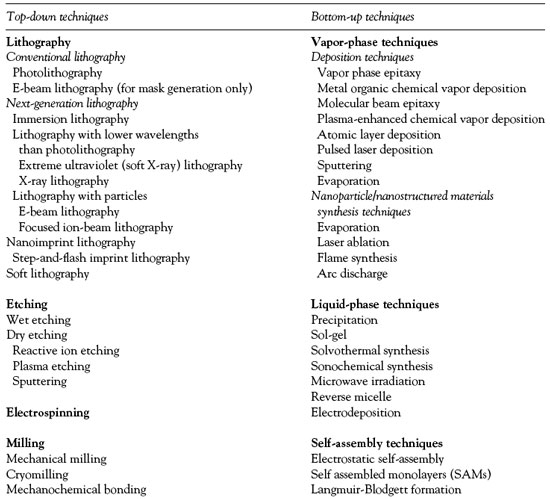
| The paper by the UIC scientists takes a detailed look at the sources of environmental impacts of current production methods for nanomaterials and they evaluate both top-down and bottom-up nanomanufacturing methods. | |
|
|
| Common nanomanufacturing methods. (Reprinted with permission from Wiley) | |
| There are a number of areas where the manufacture of nanomaterials has an environmental impact (as does all manufacturing). The question of course is if nanomaterial production leaves a larger or a smaller environmental footprint than the manufacture of traditional chemicals and products. Due to the scarcity of quantitative data with regard to energy and resource consumption as well as waste materials, this question cannot be answered conclusively. There is evidence, though, that some production processes have a considerable negative impact. Carbon nanoparticles, for instance, are found to be highly energy-intensive materials, on the order of 2 to 100 times more energy-intensive than aluminum, even with idealized production models ("Energy Requirements of Carbon Nanoparticle Production"). | |
| Or consider this: For certain one-dimensional nanoproducts, energy intensity (in terms of mass of fossil fuel use per product) is 400 times higher than that of a refrigerator and 700 times that of an automobile ("Environmental impacts of microchip manufacture"). | |
| The following is a summary of the sources of environmental impacts as identified and described by the UIC researchers. | |
| Stricter Purity Requirements and Less Tolerance for Contamination During Processing Compared to Conventional Manufacturing Processes | |
| Semiconductor devices as well as many nanomaterials require extraordinary levels of purity in terms of starting materials, water, and chemicals used during production, as well as the frequent requirement for a clean room environment. The processes to achieve the required levels of purity are energy intensive. For instance, the energy intensity of a class 1 or 10 clean room is five times higher than a class 100,000 clean room. | |
| Ultrapure water for processing requires an average of 1.4 to 1.6 gallons of potable water to obtain 1 gallon of ultrapure water. Subsequent recycling of ultrapure spent rinse water, which contains trace elements of metals, acids/bases, and solvents, poses several challenges. | |
| Low Process Yields or Material Efficiencies | |
| The authors write that, for many processes, only a small percentage of the starting materials is ultimately incorporated into final products, the rest accumulating on reactor walls (thus requiring frequent cleaning) or flowing to effluent waste streams. "Few systematic methods for recovering unused materials exist at present. Deposition, ion implantation, chamber cleaning, and dry etching techniques, for 1-D nanoproducts manufacturing, have low material or precursor utilization efficiencies, ranging from 3% to 10% for MBE and 1 to 20% for metal organic CVD." | |
| Repeated Processing, Postprocessing, or Reprocessing Steps of a Single Product or Batch | |
| One example of how high-repetition processing steps create large amounts of waste materials: "Nanoparticles extracted from solution by precipitation and centrifugation must be washed repeatedly with organic solvents and ultrapure water until the products are isolated from solvents, surfactants, or reagents. Liquid-phase synthesis techniques also require postannealing treatments to change the morphology of the products. As much as 15 liters of solvent per gram of product may be used." | |
| Modern chip production technologies require numerous processing steps that involve a significant use of chemicals, surfactants and ultrapure water. The report notes that the lithography step is the most waste-producing process during wafer processing. It is a chemically intensive process that "is characterized by both significant energy consumption (excimer lasers) and the use of chemicals (coatings and photoresist mixtures), some of which are toxic and have to be disposed of as hazardous waste." | |
| Use of Toxic, Basic, or Acidic Chemicals and Organic Solvents | |
| According to the report, it is estimated that 99.9% of materials used to manufacture one-dimensional nanoproducts are not contained in the final products. Also, "despite major reductions in energy consumption and ultrapure water use, chemical use per product and chemical waste generation have been increasing in semiconductor facilities due to increasing wafer production and more complex processes." | |
| In addition, life cycle impact analyses have not been done yet for many of the chemicals used in nanomanufacturing, so a total environmental footprint cannot be compiled yet. | |
| Need for Moderate to High Vacuum and Other Specialized Environments | |
| Many of the specialized nanomanufacturing processes are energy hogs due to demanding process requirements such as ultrahigh vacuums or high temperatures that can reach 1,000° C or more. Although deposition times during thin film production are actually quite short, deposition chambers have to be ramped up as long as 24 hours prior to deposition. | |
| Use of or Generation of Greenhouse Gases | |
| "Greenhouse gases emanate from two general sources: those generated upstream of nanostructure manufacturing (many processes have significant energy requirements, often in the form of high and/or prolonged heat), and those that are a direct result of manufacturing processes, such as the PFCs used for cleaning deposition chambers and as dry etching gases." | |
| The authors conclude that, from an examination of the attributes of existing nanomanufacturing processes, a number of efficiency and toxicity problems exist and they will need to be addressed as the field matures. What cannot be answered fully yet is whether nanotechnology manufacturing processes are more or less sustainable than 'conventional' industrial methods because life cycle comparisons have not been done yet. | |
| It also might be appropriate to look at the "Twelve Principles of Green Chemistry" that the U.S. Environmental Protection Agency has posted on its "Green Chemistry" website. Green chemistry, also known as sustainable chemistry, is the design of chemical products and processes that reduce or eliminate the use or generation of hazardous substances. The 12 principles can be fully applied to nanomanufacturing processes: | |
| 1. Prevent waste: Design chemical syntheses to prevent waste, leaving no waste to treat or clean up. | |
| 2. Design safer chemicals and products: Design chemical products to be fully effective, yet have little or no toxicity. | |
| 3. Design less hazardous chemical syntheses: Design syntheses to use and generate substances with little or no toxicity to humans and the environment. | |
| 4. Use renewable feedstocks: Use raw materials and feedstocks that are renewable rather than depleting. Renewable feedstocks are often made from agricultural products or are the wastes of other processes; depleting feedstocks are made from fossil fuels (petroleum, natural gas, or coal) or are mined. | |
| 5. Use catalysts, not stoichiometric reagents: Minimize waste by using catalytic reactions. Catalysts are used in small amounts and can carry out a single reaction many times. They are preferable to stoichiometric reagents, which are used in excess and work only once. | |
| 6. Avoid chemical derivatives: Avoid using blocking or protecting groups or any temporary modifications if possible. Derivatives use additional reagents and generate waste. | |
| 7. Maximize atom economy: Design syntheses so that the final product contains the maximum proportion of the starting materials. There should be few, if any, wasted atoms. | |
| 8. Use safer solvents and reaction conditions: Avoid using solvents, separation agents, or other auxiliary chemicals. If these chemicals are necessary, use innocuous chemicals. | |
| 9. Increase energy efficiency: Run chemical reactions at ambient temperature and pressure whenever possible. | |
| 10. Design chemicals and products to degrade after use: Design chemical products to break down to innocuous substances after use so that they do not accumulate in the environment. | |
| 11. Analyze in real time to prevent pollution: Include in-process real-time monitoring and control during syntheses to minimize or eliminate the formation of byproducts. | |
| 12. Minimize the potential for accidents: Design chemicals and their forms (solid, liquid, or gas) to minimize the potential for chemical accidents including explosions, fires, and releases to the environment. | |
 By
Michael
Berger
– Michael is author of three books by the Royal Society of Chemistry:
Nano-Society: Pushing the Boundaries of Technology,
Nanotechnology: The Future is Tiny, and
Nanoengineering: The Skills and Tools Making Technology Invisible
Copyright ©
Nanowerk LLC
By
Michael
Berger
– Michael is author of three books by the Royal Society of Chemistry:
Nano-Society: Pushing the Boundaries of Technology,
Nanotechnology: The Future is Tiny, and
Nanoengineering: The Skills and Tools Making Technology Invisible
Copyright ©
Nanowerk LLC
|
Become a Spotlight guest author! Join our large and growing group of guest contributors. Have you just published a scientific paper or have other exciting developments to share with the nanotechnology community? Here is how to publish on nanowerk.com.