| Posted: Jan 12, 2009 | |
Nano-welding facilitates bottom-up nanotechnology fabrication |
|
| (Nanowerk Spotlight) Civilization as we know it would, literally, fall apart without techniques to join materials together. With its historic development tracing back to the Bronze Age, welding has been one of the key technologies that serves modern industry in broad areas such as construction, manufacturing, and engineering. As we have reported in a previous Nanotechnology Spotlight, this Bronze Age technique could prove very useful in building complex nanostructures. | |
| Researchers at the University of Sheffield in the UK have now demonstrated the ability to reliably weld individual nanowires and nanoobjects into complex geometries with controllable junctions. This represents a significant breakthrough for the current and future bottom-up localized assembly, integration, and repair of micro- and nanodevices. | |
| "Most everyday joining techniques cannot be applied at the nanoscale, where nano-objects are easily destroyed by heat," Dr. Beverley Inkson tells Nanowerk. "Scientists have developed many ways to make individual nano-objects, but not many ways to securely join them together. But now we have reached a point where the ability to weld individual nanoscale objects such as nanowires and nanoparticles together is becoming vitally important for nanotechnology applications such as nanosensors and nanoelectronics." | |
| Inkson is a Reader in Nanostructured Materials at the University of Sheffield's NanoLAB and Chair of the UK NanoFIB network. As part of the RCUK Basic Technology programme in Nanorobotics, where Inkson is project director, she and her team (post doc researcher Yong Peng and Professor Tony Cullis) have developed a new way to weld together individual nanowires and nano-objects using tiny blobs of metal solder less than 250 atoms across. | |
| This nanoscale electrical welding technique radically improves the spatial resolution, flexibility, and controllability of welds between individual nanowires and nanoobjects. Inkson notes that the key advance is to avoid detrimental current flow though the nanoobjects to be joined and instead to locally deposit nanoscale volumes of a chosen metal at the weld site by Joule heating a sacrificial nanowire. | |
| "The nanosolder is deposited by heating a tiny metal wire in contact with the materials to be joined," explains Inkson. "The solder wire melts and flows onto the join. The welding can be watched in real-time inside an electron microscope, allowing the choice of exactly where, and how much, nanosolder is deposited." | |
 |
|
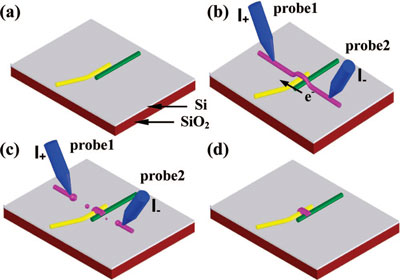
| Schematic of nanoconstruction by the welding of individual nanoobjects (nanowires) using nanoscale solder. (a) Assembly of individual nanoobjects into a desired pattern using a nanomanipulator probe. (b) Placement of a sacrificial nanowire in contact with the nanostructure to be welded. (c) Nanowelding the nanoobjects together by an electrical signal. (d) Completed nanoweld. (Reprinted with permission from the American Chemical Society) | |
| The use of nanosolder is particularly exciting because the strength and conductivity of the join can be engineered at the nanoscale by controlling the chemistry, structure, and volume of solder material used. | |
| The Sheffield team demonstrated the soldering of nanoobjects into complex networks by two examples which illustrate the wide applicability and performance of the technique. | |
| In the first example, they welded 55 nm gold nanowires with gold solder into complex patterns, including triple junctions, which cannot be achieved by direct Joule heating of the nanowires due to morphological instabilities induced by current flow. | |
| "The ability to weld gold nanowires is important since, due to their excellent electrical conductivity and stability in oxidizing environments, they are widely used for electrodes and interconnects in the semiconductor industry and nanoelectronics research," says Inkson. | |
 |
|
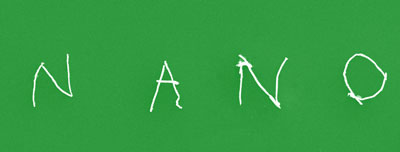
| Nanoconstruction using nanoscale solder. The word 'NANO' is written by individual 55nm diameter gold nanowires. (Adapted from Figure 2, Nano Letters, ASAP Article, DOI:10.1021/nl8025339) | |
| In the second example, the researchers demonstrated that dissimilar nanowires can be welded together, using a third material as solder. They specifically chose gold-tin alloy solder – widely used in macroscopic welding due to its excellent conductivity, low melting point, and large corrosion resistance – to result in an ultralow electrical resistance join between nanowires. | |
| According to Inkson, the ability to integrate functional nanowires into circuits via high-performance welded joins represents a significant advance for nanoscale sensor development. Furthermore, an immediate check of nanoweld quality is essential for practical nanoconstruction, and this can be done in situ directly after welding. | |
| The new nanowelding technique can be used to join nano-objects with a wide range of shapes and chemistries, and so could be used in the future as part of a 3D nanoscale fabrication line. Nanosolder can also rejoin things that have come apart during use, such as interconnect wires in computer chips which often fail by the formation of holes (by 'electromigration'). | |
| Nanosolder has immediate research and industrial applications including fabrication of multifunctional nanosensors and nanoelectronics constructed from a small number of nanoobjects, and repair of interconnects and failed nanoscale electronics. | |
| The team has reported their findings in the December 10, 2008 online edition of Nano Letters ("Bottom-up Nanoconstruction by the Welding of Individual Metallic Nanoobjects Using Nanoscale Solder"). | |
 By
Michael
Berger
– Michael is author of three books by the Royal Society of Chemistry:
Nano-Society: Pushing the Boundaries of Technology,
Nanotechnology: The Future is Tiny, and
Nanoengineering: The Skills and Tools Making Technology Invisible
Copyright ©
Nanowerk LLC
By
Michael
Berger
– Michael is author of three books by the Royal Society of Chemistry:
Nano-Society: Pushing the Boundaries of Technology,
Nanotechnology: The Future is Tiny, and
Nanoengineering: The Skills and Tools Making Technology Invisible
Copyright ©
Nanowerk LLC
|
|
|
Become a Spotlight guest author! Join our large and growing group of guest contributors. Have you just published a scientific paper or have other exciting developments to share with the nanotechnology community? Here is how to publish on nanowerk.com. |
|