| Posted: Feb 02, 2009 | |
One route to nanomanufacturing leads through nanocrystal synthesis |
|
| (Nanowerk Spotlight) In order for bottom-up nanomanufacturing to become a reliable technology that can be scaled up to industrial processes, researchers need to make significant improvements in the way the nanoscale building blocks for creating structures and devices are created. Since nanomanufacturing takes place at length scales of billionths of a meter, the required degree of precision is at the same scale – differences of a few nanometers could determine if a device works or not. | |
| In contrast to nanorobotic assembly, which in principle bears some resemblance to the industrial assembly line manufacturing we see in factories today, current nanomanufacturing research and development heavily depends on nature's way of building things – through growing it. For instance, a large body of research has developed in the area of nanocrystals, or quantum dots. These crystals, because of what is called the quantum confinement effect, offer a powerful means of tuning the electronic, optical, and magnetic properties of a solid material. | |
| The properties of a quantum dot are not only determined by its size but also by its shape, composition, and structure, for instance if it's solid or hollow. A reliable manufacturing technology that makes use of nanocrystals' properties – for a wide-ranging number of applications in such areas as catalysis, electronics, photonics, information storage, imaging, medicine, or sensing – needs to be capable of churning out large quantities of nanocrystals where each batch is produced according to the exactly same parameters. | |
| In a recent review article in ACSNano, Sara Skrabalak from Indiana University and Younan Xia from Washington University in St. Louis, describe recent advances in seeded growth as the ultimate approach to producing metal nanocrystals with precisely controlled sizes, shapes, and compositions – the necessary first step toward their use and assembly for large-scale applications ("Pushing Nanocrystal Synthesis toward Nanomanufacturing"). | |
| "With these tools in hand, countless multifunctional nanocrystals can be envisioned and synthetically targeted" adds Skrabalak. "Additionally, as the size distribution associated with nanocrystals prepared by a seeded growth method is generally narrow, their assembly into larger structures and devices may be possible, having been recently demonstrated for both silver nanocubes and nanorods. The continued development of synthetic routes to increasingly multidimensional building blocks and their assembly into functional structures marks the next and critical stage in nanomanufacturing." | |
| Surprising as it may sound, the first solution-phase synthesis of metal nanocrystals can actually be traced back to the 1850s when Michael Faraday prepared stable gold colloids by reducing gold chloride with phosphorus in water. Since then, many different methods have been developed for preparing nanocrystals of various compositions. | |
| In their article, Skrabalak and Xia describe how the problems with early work – widely distributed sizes, poorly defined shapes, and limited structures – were overcome step by step. | |
| "A conceptual breakthrough in nanocrystal synthesis came when it was realized that the shape taken by nanocrystals produced in a solution phase directly correlated to the twinned structure of the seeds present in the synthesis," says Xia. "The variation in shape that originates from the same type of seed can be attributed to the degree to which a particular crystal facet is stabilized by the capping agent (i.e., polymers or ionic species involved in a synthesis). Thus, in order to prepare one type of metal nanocrystal to the exclusion of others, both the structure of the seed present in solution and the capping ability of solution additives must be controlled." | |
 |
|
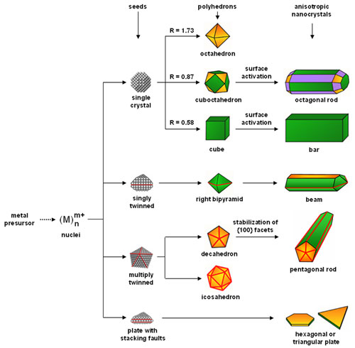
| Schematic illustrating the correlations between seeds in single crystal, singly twinned, multiply twinned, and plate-like structures and nanocrystals of face-center-cubic metals with different shapes. Twin plains are delineated in the drawing with red lines. The green, orange, and purple colors represent the {100}, {111}, and {110} facets, respectively. The parameter R is defined as the ratio between the growth rates along the (100) and (111) direction. (Reprinted with permission from Wiley) | |
| One of the major challenges to the synthesis of metal nanocrystals has been controlling the population of the various types of seeds involved in a synthesis. "In many cases, a mixture of single-crystal, singly twinned, and multiply twinned seeds are present" says Skrabalak. "However, by manipulating reaction kinetics and exploiting processes such as oxidative etching, it is now possible to generate exclusively one type of seed over the others." | |
| She points out that, with the role of seeds better understood, it also becomes possible to use seeds with well- defined shapes to obtain increasingly complex nanocrystals that would otherwise be inaccessible by solution-phase methods. Several examples in the review illustrate how seeded growth techniques are enabling the integration of multiple features into one nanostructure. | |
| "Recent research is showing how seeded growth is facilitating the preparation of multicomponent nanocrystals with complex and highly tunable structures" says Xia. "While in our review we have focused on the seeded growth of metal nanocrystals, a similar approach has also been used to increase the quality and functionality of metal oxide and metal chalcogenide nanocrystals. In particular, there has been a growing interest in constructing nanocrystals that incorporate both semiconductor and metal components (e.g., cadmium selenide - gold hybrids) into well-organized arrangements." | |
| "Seeded growth has a long history in material science, and with the advent of nanotechnology, it has emerged as a powerful means of precisely controlling the size, shape, composition, and yield of nanocrystals prepared using solution-phase methods" he says. "We anticipate that its use will continue to grow as both new types of seeds are generated and as methods for controlling the nonconformal deposition are developed." | |
 By
Michael
Berger
– Michael is author of three books by the Royal Society of Chemistry:
Nano-Society: Pushing the Boundaries of Technology,
Nanotechnology: The Future is Tiny, and
Nanoengineering: The Skills and Tools Making Technology Invisible
Copyright ©
Nanowerk LLC
By
Michael
Berger
– Michael is author of three books by the Royal Society of Chemistry:
Nano-Society: Pushing the Boundaries of Technology,
Nanotechnology: The Future is Tiny, and
Nanoengineering: The Skills and Tools Making Technology Invisible
Copyright ©
Nanowerk LLC
|
|
|
Become a Spotlight guest author! Join our large and growing group of guest contributors. Have you just published a scientific paper or have other exciting developments to share with the nanotechnology community? Here is how to publish on nanowerk.com. |
|