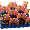
 Researchers have proposed a strategy to grow 'face-on' and 'edge-on' conductive metal-organic frameworks (cMOF) nanofilms on substrates by controlling the 'stand-up' behaviors of ligands on various surfaces to overcome the difficulty in the orientation control of such film.
Oct 9th, 2023
Read more
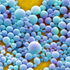
 Using micro-engineered soil models, researchers have investigated the effect of tiny polystyrene particles on bacteria and fungi. While these nanoplastics reduced both bacterial and fungal growth, the fungus actually managed to 'clean up' their surroundings, thereby easing the effect of the plastics.
Oct 9th, 2023
Read more
 Combining a bulky chain with a stable polymer can enhance liquid crystal performance.
Oct 9th, 2023
Read more
 Perovskite-based solar cells are viewed as potential successors to the prevalent silicon cells because of their cost-effectiveness and outstanding performance. Recent research has showcased perovskite photovoltaic cells with enhanced optoelectronic properties. One of the main obstacles to their wider adoption is reducing optical losses in these next-generation cells.
Oct 6th, 2023
Read more
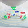
 Researchers accelerated the reaction between cancer cell-derived nanoparticles and antibody-modified microparticles using laser light. The 3D structure of the aggregates was analyzed with a confocal optical system. Results showed the capability to measure 1,000 to 10,000 nanoscale extracellular vesicles in a 500 nL sample within 5 minutes.
Oct 6th, 2023
Read more
 Researchers explore twisted graphene's unique properties using a tool to measure electron energy levels, paving the way for electronics and new resistance standards.
Oct 5th, 2023
Read more
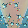
 Researchers created a novel electron-spin qubit platform, assembled atom-by-atom on a surface.
Oct 5th, 2023
Read more
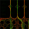
 Defects can make a material stronger or make it fail catastrophically; Knowing how fast they travel can help researchers understand things like earthquake ruptures, structural failures and precision manufacturing.
Oct 5th, 2023
Read more
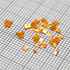
 Development of Surface-Enhanced Raman Scattering (SERS) and machine learning based methods for on-site applicable, facile, and rapid detection of microplastics.
Oct 5th, 2023
Read more
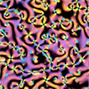
 Scientists successfully observed the left and right handedness of material structures at the nanoscale, by illuminating chiral gold nanostructures with circularly polarized light and detecting the optical force acting on a probe near the nanostructures. This result demonstrated that it is possible to analyze the chiral structure of matter at the nanoscale using light.
Oct 5th, 2023
Read more
 Picture a smartphone clad in a casing that's not just for protection but also doubles as a reservoir of electricity, or an electric car where the doors and floorboard store energy to propel it forward.
Oct 5th, 2023
Read more
 Researchers successfully morphed all-inorganic perovskites at room temperature without compromising their functional properties. Their findings demonstrate the potential of this class of semiconductors for manufacturing next-generation deformable electronics and energy systems in the future.
Oct 5th, 2023
Read more
 Study shows a promising strategy to reduce adverse reactions to nanoparticles by using complement inhibitors.
Oct 5th, 2023
Read more
 Researchers developed a semiconductor that efficiently generates light and simultaneously gives that light a certain spin. This chiral perovskite material has great technological potential that can be used for applications in optoelectronics, telecommunications, and information processing.
Oct 5th, 2023
Read more
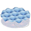
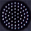 The new technique uses a 3D laser to ablate a curved surface, followed by etching in acid. This method can produce high-quality 3D concave lens arrays that can be used to make soft compound eyes. Image restoration using a deep learning algorithm can further improve image quality.
Oct 5th, 2023
Read more
 A new review discusses laser-scribed graphene for sensor fabrication.
Oct 5th, 2023
Read more
 Subscribe to our Nanotechnology News feed