Metamaterial absorbers for infrared inspection technologies
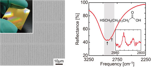 A metamaterial absorber capable of highly sensitive infrared detection enhances the spectroscopy of tiny molecular details.
Sep 28th, 2015
Read moreA metamaterial absorber capable of highly sensitive infrared detection enhances the spectroscopy of tiny molecular details.
Sep 28th, 2015
Read more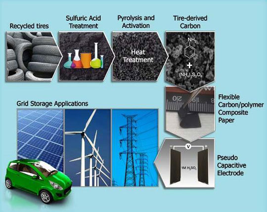 Some of the 300 million tires discarded each year in the United States alone could be used in supercapacitors for vehicles and the electric grid using a new technology.
Sep 25th, 2015
Read more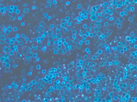 To the growing list of two-dimensional semiconductors, such as graphene, boron nitride, and molybdenum disulfide, whose unique electronic properties make them potential successors to silicon in future devices, you can now add hybrid organic-inorganic perovskites. However, unlike the other contenders, which are covalent semiconductors, these 2D hybrid perovskites are ionic materials, which gives them special properties of their own.
Sep 25th, 2015
Read more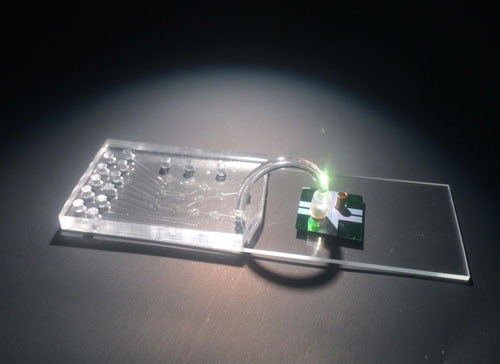 Hybrid device integrates a microfluidic chip for sample preparation and an optofluidic chip for optical detection of individual molecules of viral RNA.
Sep 25th, 2015
Read more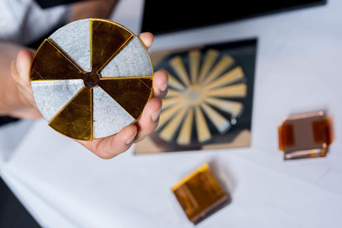 To provide a means for both comparing and selecting these energy-harvesting nanogenerators for specific applications, the Georgia Institute of Technology research group that pioneered the triboelectric nanogenerator (TENG) technology has now proposed a set of standards for quantifying device performance. The proposal evaluates both the structural and materials performance of the four major types of TENG devices.
Sep 25th, 2015
Read more Two-dimensional organic lattices are easier and safer to work with than inorganic materials for spintronic and quantum computing applications.
Sep 25th, 2015
Read moreImperfections running through liquid crystals can be used as miniscule tubing, channeling molecules into specific positions to form new materials and nanoscale structures.
Sep 25th, 2015
Read more Ultrafast laser pulses can manipulate 'bubble' domains for future spintronic and logic devices.
Sep 25th, 2015
Read more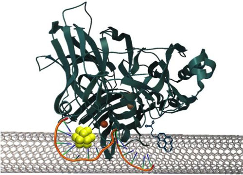 New technique removes barrier to development of biofuel cells with efficient performance.
Sep 24th, 2015
Read more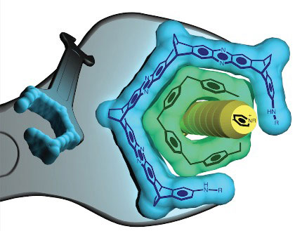 Scientists have invented a new way to use chirality to make a wrench. A nanoscale wrench. The discovery allows to precisely control nanoscale shapes and holds promise as a highly accurate and fast method of creating customized molecules.
Sep 24th, 2015
Read more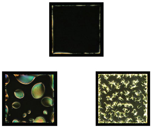 Researchers are putting liquid crystals to work in a completely unexpected realm: as detectors for the protein fibers implicated in the development of neuro-degenerative diseases such as Alzheimer's.
Sep 24th, 2015
Read more A detailed nanomechanical study of mechanical degradation processes in silicon structures containing varying levels of lithium ions offers good news for researchers attempting to develop reliable next-generation rechargeable batteries using silicon-based electrodes.
Sep 24th, 2015
Read more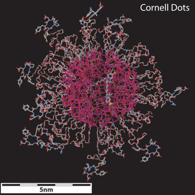 Cornell University, in partnership with Memorial Sloan Kettering Cancer Center, is opening a new $10 million Center of Cancer Nanotechnology Excellence that brings together scientists, engineers, biologists and physicians to develop and translate new cancer care applications based on nanotechnology.
Sep 24th, 2015
Read more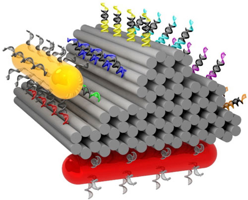 A tiny gold rod walks across a surface guided by DNA and can be tracked step by step.
Sep 24th, 2015
Read more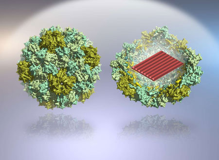 Self-assembled DNA nanostructures can be used in molecular-scale diagnostics and as smart drug-delivery vehicles.
Sep 24th, 2015
Read more Crucial to silicon semidconductor applications is the ability to 'dope' the semiconductor; which is to say, by controllably adding impurity atoms to a semiconductor, one can continuously vary its electronic and optical properties. Scientists now have demonstrated for the first time, a unique nanoscale analogue.
Sep 24th, 2015
Read more Subscribe to our Nanotechnology News feed