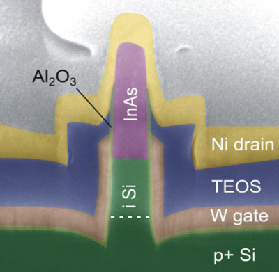
 Researchers found that by adding a specific atomic thin film layer to a transistor, the layer acted as a filter for the energy that passed through it at room temperature. The signal that resulted from the device was six to seven times steeper than that of traditional devices. Steep devices use less voltage but still have a strong signal.
Sep 26th, 2014
Read more
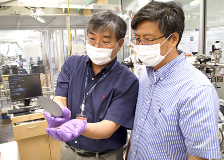
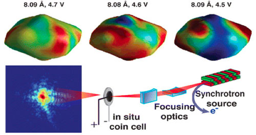 A new method developed for studying battery failures points to the potential next step in extending lithium ion battery lifetime and capacity, opening a path to wider use of these batteries in conjunction with renewable energy sources.
Sep 26th, 2014
Read more
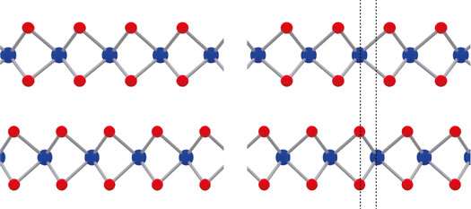 Harnessing an unusual 'valley' quantum property of electrons offers a new possibility for next-generation electronics.
Sep 26th, 2014
Read more
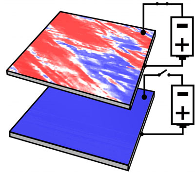 Electricity and magnetism rule our digital world. Semiconductors process electrical information, while magnetic materials enable long-term data storage. A research team has discovered a way to fuse these two distinct properties in a single material, paving the way for new ultrahigh density storage and computing architectures.
Sep 25th, 2014
Read more
 The various patterns that atoms of a solid material can adopt, called crystal structures, can have a huge impact on its properties. Being able to accurately predict the most stable crystal structure for a material has been a longstanding challenge for scientists. Researchers calculated the lattice energy of benzene, a simple yet important molecule in pharmaceutical and energy research, to sub-kilojoule per mole accuracy - a level of certainty that allows polymorphism to be resolved.
Sep 25th, 2014
Read more
 New experimental results have revealed the critical influence of the electronic and geometric effects in the carbon dioxide reduction reaction.
Sep 25th, 2014
Read more
Analysis of material's molecular structure leads to a new formula that could cut greenhouse-gas emissions.
Sep 25th, 2014
Read more
 Gallium arsenide a semiconductor composed of gallium and arsenic is well known to have properties that promise practical applications. In the form of nanowires it has particular potential for use in solar cell manufacture and optoelectronics in many of the same applications that silicon is commonly used. But its natural semiconducting ability requires tuning to make it more desirable for use in manufacturing. New work offers a novel approach to such tuning.
Sep 25th, 2014
Read more
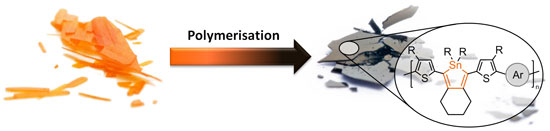 Semiconducting polymers can be used, for example, for the absorption of sun light in solar cells. By incorporating organic tin into the plastic, light can be absorbed over a wide range of the solar spectrum.
Sep 25th, 2014
Read more
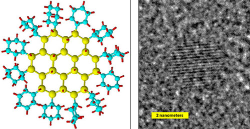 NIST recently issued Reference Material (RM) 8027, the smallest known reference material ever created for validating measurements of these man-made, ultrafine particles between 1 and 100 nanometers in size.
Sep 25th, 2014
Read more
 The European project E2SWITCH is aiming to develop new electronic systems with ultra-low energy consumption. The nine partners, universities, research institutes and companies, are committed to making these 'circuits of tomorrow' more energy efficient.
Sep 25th, 2014
Read more
In a step that could lead to longer battery life in smartphones and lower power consumption for large-screen televisions, researchers have extended the lifetime of blue organic light emitting diodes by a factor of 10.
Sep 25th, 2014
Read more
 A novel type of reso�nant cavity serves as a prison for photons. The cavity confines light in all three dimensions in space inside a photonic crystal. The crystals have a struc�ture similar to how atoms are arranged in diamond gems.
Sep 25th, 2014
Read more
 Scientists investigated the structural and optical properties of silicon nanowires synthesized by metal-assisted chemical etching.
Sep 25th, 2014
Read more
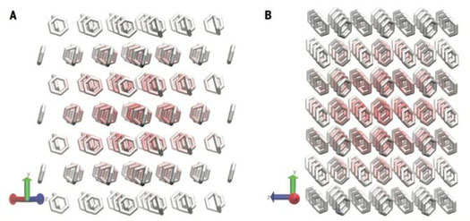
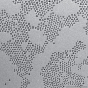
 Researchers exploit the self-organization of semiconducting nanocrystals by the Stranski-Krasnov (SK) mode of crystal growth for producing ordered, highly dense, and highly uniform quantum dots. This bottom-up approach yields much better results than the conventional photolithographic or top-down methods widely used for the fabrication of nanostructures.
Sep 25th, 2014
Read more
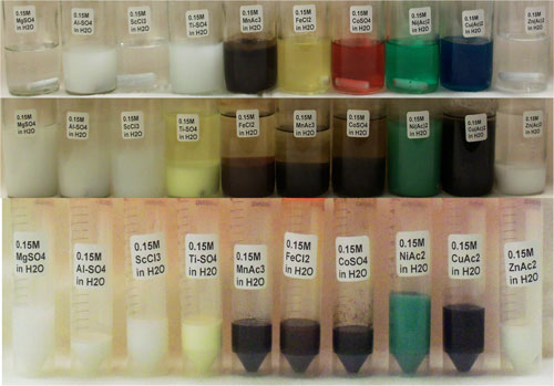 Scientists have developed a novel one-step process using, for the first time in these types of syntheses, potassium superoxide to rapidly form oxide nanoparticles from simple salt solutions in water.
Sep 24th, 2014
Read more
 Subscribe to our Nanotechnology News feed