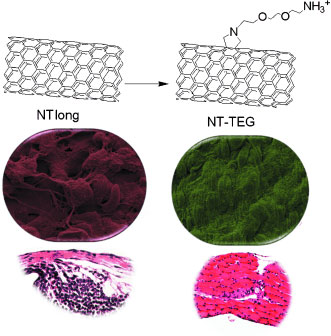
 Carbon nanotubes resemble asbestos fibers in their form. Unfortunately, long, pure nanotubes also seem to have asbestos-like pathogenicity. A European research team has now reported that chemical modifications can alleviate this problem if the modification makes their surface more water-friendly and reduces the effective length of the tubes.
Jan 21st, 2013
Read more
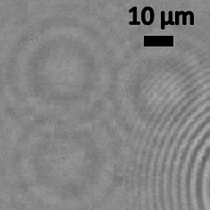 By using tiny liquid lenses that self-assemble around microscopic objects, a team from UCLA's Henry Samueli School of Engineering and Applied Science has created an optical microscopy method that allows users to directly see nanoscale objects.
Jan 21st, 2013
Read more
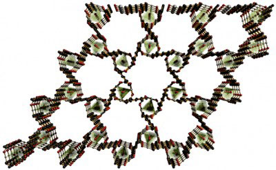 Reseaerchers have developed a highly-porous Metal Organic Framework (MOF) that, almost uniquely, is stable and able to filter substances in water.
Jan 21st, 2013
Read more
Researchers will explore new materials and atomic-scale structures for more powerful and energy-efficient semiconductor components.
Jan 21st, 2013
Read more
Ceramic forms of hydrophobic materials could be far more durable than existing coatings or surface treatments.
Jan 21st, 2013
Read more
 Quantitative nanoindentation experiments showed an increase of yield strength from 1.64 to 2.29 GPa during the multiple loading-unloading cycles. Their study provides both the evidence to explain the roots of work hardening at small length scales and the insight for future design of ductile nanocrystalline metals.
Jan 19th, 2013
Read more
Taiwan's National Applied Research Laboratories (NARL) will launch a platform on Jan. 22 to further promote nanotechnology in the private and academic sectors, according to the organizers.
Jan 19th, 2013
Read more
$28 million grant to fund 'Center for Spintronic Materials, Interfaces and Novel Architectures,' aimed at supporting US semiconductor industry.
Jan 18th, 2013
Read more
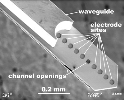 Scientists build a microimplant that uses a laser to control individual nerve cells.
Jan 18th, 2013
Read more
 Over three days in December, four research groups announced progress on a quantum-computing proposal made two years ago by MIT researchers.
Jan 18th, 2013
Read more
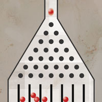
Researchers from the NIST Center for Nanoscale Science and Technology and the Johns Hopkins University have developed a technique to reliably manipulate hundreds of individual micrometer-sized colloid particles to create crystals with controlled dimensions.
Jan 18th, 2013
Read more
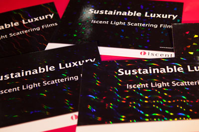 New features for consumer products with eye-catching, communicative and ecological packaging.
Jan 18th, 2013
Read more
New findings are the first to show that it really is possible to use nanowires to manufacture solar cells.
Jan 18th, 2013
Read more
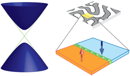 A new class of magnets where fewer electrons mean stronger magnetism could lead to new energy-saving technologies.
Jan 18th, 2013
Read more
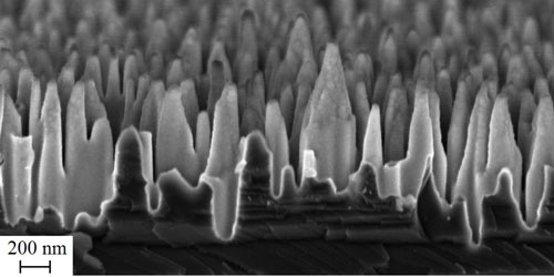 Scientists at Aalto University, Finland, have demonstrated results that show a huge improvement in the light absorption and the surface passivation on silicon nanostructures. This has been achieved by applying atomic layer coating.
Jan 18th, 2013
Read more
Almost 100 years after the initial discovery, a team of scientists at the University of Alberta and the National Institute for Nanotechnology in Edmonton have harnessed the Barkhausen Effect as a new kind of high-resolution microscopy for the insides of magnetic materials.
Jan 17th, 2013
Read more
 Subscribe to our Nanotechnology News feed