Breakthrough nanoparticle halts multiple sclerosis
New nanotechnology can be used for Type 1 diabetes, food allergies and asthma.
Nov 18th, 2012
Read moreNew nanotechnology can be used for Type 1 diabetes, food allergies and asthma.
Nov 18th, 2012
Read moreTo help planes fly safely through cold, wet, and icy conditions, a team of Japanese scientists has developed a new super water-repellent surface that can prevent ice from forming in these harsh atmospheric conditions. Unlike current inflight anti-icing techniques, the researchers envision applying this new anti-icing method to an entire aircraft like a coat of paint.
Nov 17th, 2012
Read moreSmall floating objects change the dynamics of the surface they are on. This is an effect every serious student of breakfast has seen as rafts of floating cereal o's arrange and rearrange themselves into patterns on the milk. Now scientists have suggested that this process may offer insight into nanoscale engineering processes.
Nov 17th, 2012
Read more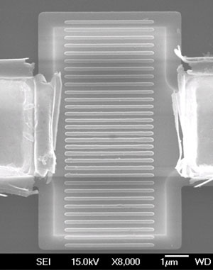 Rice University lab produces microscopic devices for fast manipulation of incident infrared light.
Nov 16th, 2012
Read moreBy tweaking the formula for growing oxide thin films, researchers at the Department of Energy's Oak Ridge National Laboratory achieved virtual perfection at the interface of two insulator materials.
Nov 16th, 2012
Read moreA fundamental cornerstone for spintronics that has been missing up until now has been constructed by a team of physicists at Link�ping University in Sweden. It's the world's first spin amplifier that can be used at room temperature.
Nov 16th, 2012
Read more With an amount of 51 million it is one of the largest ever Dutch investments in fundamental science: scientists of TU Delft and Leiden University will be embarking on the research programme 'NanoFront' to explore the frontiers of nanoscience in the coming ten years.
Nov 16th, 2012
Read moreUniversity of Glasgow scientists have helped to create silicon optical chips to generate twisted beams of light which could be used to manipulate tiny particles or increase the capacity of optical communications technology.
Nov 16th, 2012
Read moreRichard Overill of the Department of Informatics at King's College London is working in the field of digital forensics to develop the necessary tools to pre-empt the cyber-criminals as quantum computing becomes reality.
Nov 16th, 2012
Read more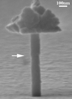 In order to build the next generation of nuclear reactors, materials scientists are trying to unlock the secrets of certain materials that are radiation-damage tolerant. Now researchers at the California Institute of Technology (Caltech) have brought new understanding to one of those secrets - how the interfaces between two carefully selected metals can absorb, or heal, radiation damage.
Nov 16th, 2012
Read moreRealizes a room temperature operation switching transistor by helium ion irradiation.
Nov 16th, 2012
Read more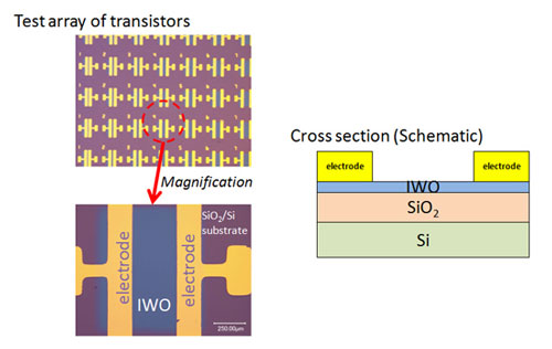 Next-generation device enabling improved smartphone battery life and high definition in televisions.
Nov 16th, 2012
Read moreDie Bundesanstalt f�r Arbeitsschutz und Arbeitsmedizin (BAuA) hat den Forschungsauftrag zur "Charakterisierung von nanoskaligen Eigenschaften chemischer Stoffe als Grundlage f�r die Regulierung im Rahmen der Verordnung (EG) Nr. 1907/2006 (REACH)" vergeben. Der jetzt ver�ffentlichte Endbericht zeigt, wie sich die f�r die REACH-Verordnung geltenden physikalisch-chemischen Pr�fnachweise auf Nanomaterialien anwenden lassen.
Nov 16th, 2012
Read moreResearchers discover technique to kick a record number of electrons out of an atom with an X-ray laser
Nov 16th, 2012
Read more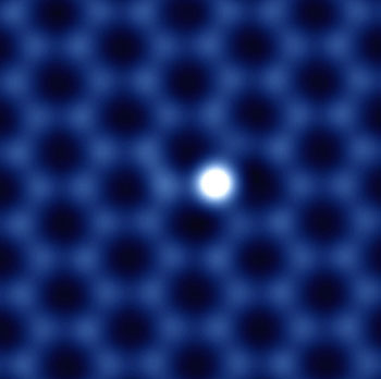 Electron microscopy at the Department of Energy's Oak Ridge National Laboratory is providing unprecedented views of the individual atoms in graphene, offering scientists a chance to unlock the material's full potential for uses from engine combustion to consumer electronics.
Nov 16th, 2012
Read moreThe remarkable properties and subsequent applications of graphene have been well-documented since it was first isolated in 2004; however, researchers are still trying to find a quick, cheap and efficient way of measuring its thickness. A group of researchers from China appear to have solved this problem by devising a universal method using just a standard optical microscope.
Nov 16th, 2012
Read more Subscribe to our Nanotechnology News feed