 A University of Arkansas physicist and his colleagues have examined the challenges facing scientists building the next generation of materials and innovative electronic devices and identified opportunities for taking the rational material design in new directions.
Jan 25th, 2012
Read more
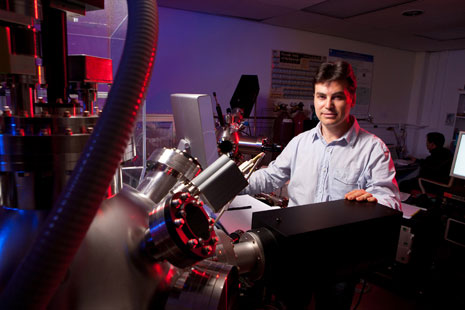
 At the Molecular Foundry, Berkeley Lab's acclaimed nanotechnology research center, Ren has pushed his Zeiss Libra 120 Cryo-Tem microscope to resolutions never envisioned by its German manufacturers, producing detailed snapshots of individual molecules. Today, he and his colleague Lei Zhang are reporting the first 3-D images of an individual protein ever obtained with enough clarity to determine its structure.
Jan 24th, 2012
Read more
Orbit of captured electron matches orbit of Jupiter's captured asteroids.
Jan 24th, 2012
Read more
Ultraviolet radiation is the catalyst for cellular damage in phytoplankton.
Jan 24th, 2012
Read more
Research by UC Riverside-led team has potential applications in digital and infrared technologies.
Jan 24th, 2012
Read more
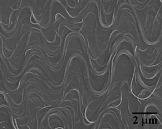 Researchers from North Carolina State University have developed a new method for creating elastic conductors made of carbon nanotubes, which will contribute to large-scale production of the material for use in a new generation of elastic electronic devices.
Jan 24th, 2012
Read more
A Rice University research team makes graphene suitable for a variety of organic chemistry applications.
Jan 24th, 2012
Read more
Gesucht: die innovativsten Nanotechnologie-Demonstrationsversuche.
Jan 24th, 2012
Read more
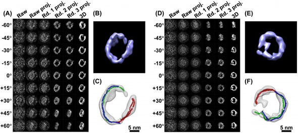
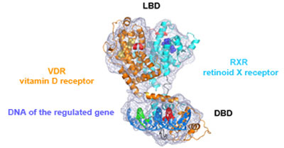 For the first time, researchers have obtained a high-resolution, full 3D image of a small but vital molecule locked up within our cells: the vitamin D receptor.
Jan 24th, 2012
Read more
Welcome to Nanoscience helps biology, chemistry, and Earth science teachers introduce the revolutionary fields of nanoscience and nanotechnology to high school students through the unique framework of the environment, specifically groundwater pollution.
Jan 24th, 2012
Read more
By using a novel technique to better understand mineral growth and dissolution, researchers at the Department of Energy's Oak Ridge National Laboratory are improving predictions of mineral reactions and laying the groundwork for applications ranging from keeping oil pipes clear to sequestering radium.
Jan 24th, 2012
Read more
The integration of electronics with materials opens up a world of possibilities, the surface of which is just being scratched.
Jan 24th, 2012
Read more
Developing a technology and selling a product are two very different processes, which require very different skill sets. The EU is supporting commercial exploitation of scientific results in nanotechnologies.
Jan 24th, 2012
Read more
Today, at the Electronics Park in Salina, U.S. Senator Charles E. Schumer joined APIC CEO Dr. Raj Dutt and other officials for a tour of the facility that will be renovated to make way for a nanotechnology chip foundry that could bring 200 high-tech jobs to Syracuse.
Jan 23rd, 2012
Read more
Cornell engineers, trying to better understand this process, have discovered that nanoscale voids behave differently than the larger ones that are hundreds of thousands of atoms in scale, studied through traditional physics. This insight could lead to improved ability to predict how cracks grow in metals, and how to engineer better materials.
Jan 23rd, 2012
Read more
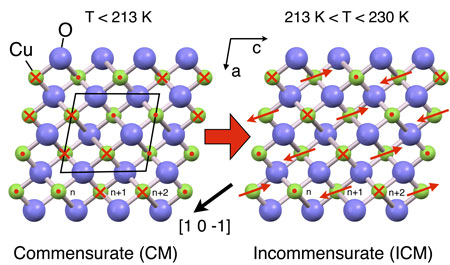 In first-of-their-kind experiments performed at the American X-ray laser LCLS, a collaboration led by researchers from the Paul Scherrer Institute has been able to precisely follow how the magnetic structure of a material changes. The study was carried out on cupric oxide (CuO).
Jan 23rd, 2012
Read more
 Subscribe to our Nanotechnology News feed