Stacking graphene layers
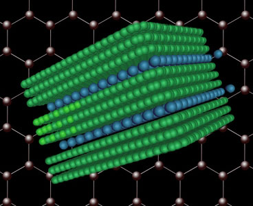 Method holds promise for making two- or three-tier graphene films that could be used for new electronic devices.
Jun 28th, 2011
Read moreMethod holds promise for making two- or three-tier graphene films that could be used for new electronic devices.
Jun 28th, 2011
Read moreScientists have discovered fundamental steps of charging of nano-sized water droplets and unveiled the long-sought-after mechanism of hydrogen emission from irradiated water.
Jun 27th, 2011
Read morePhysicists working at the University of California, Santa Barbara and the University of Konstanz in Germany have developed a breakthrough in the use of diamond in quantum physics, marking an important step toward quantum computing.
Jun 27th, 2011
Read moreThe ENIAC Joint Undertaking launched today its new Call for proposals, boosted by the strong participation of the funding authorities who committed in 2011 grants up to 175 million euros, an increase of 100% over the previous year.
Jun 27th, 2011
Read more Today, Open Access publisher InTech launches its new groundbreaking Journal, the Nanomaterials and Nanotechnology Journal, available to access online, download free of charge, and submit material without publishing fees.
Jun 27th, 2011
Read more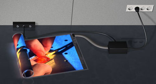 Researchers develop method to simulate customized OLEDs.
Jun 27th, 2011
Read moreSaeulen aus Galliumarsenid sind eine Alternative zu Schichten, denn sie wachsen auch auf Silizium in guter Qualitaet. Forscher des Paul-Drude-Instituts konnten jetzt den Nachweis erbringen, dass der haeufig verwendete Goldkatalysator die Eigenschaften der Saeulen empfindlich stoert.
Jun 27th, 2011
Read moreTwo new cross-disciplinary courses developed through undergraduate education research at the University of Cincinnati provide hands-on experience to better meet the growing demand for 2,000,000 nanotechnology workers that current projections hold to be needed by 2020.
Jun 27th, 2011
Read more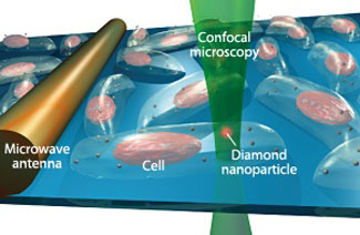 Researchers from the University of Melbourne in Australia have developed a diamond nanoparticle-based method that allows the position and orientation of the fluorescent particles to be monitored in living cells.
Jun 27th, 2011
Read more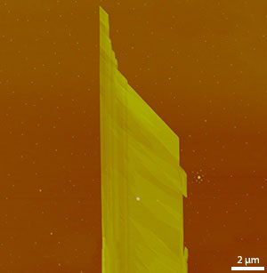 Cleaving organic crystals with adhesive tape reveals that charge carrier mobility dramatically increases below a critical thickness.
Jun 27th, 2011
Read moreRevolutionary low-power logic systems that will perform instant on/off logic operations are being developed by research scientists at the University of Southampton in partnership with the National Institute for Materials Science (NIMS), Japan, and Hitachi Cambridge Laboratory.
Jun 27th, 2011
Read more Rensselaer Polytechnic Institute engineer will study the impacts of microgravity on dangerous bacteria.
Jun 27th, 2011
Read more The novel material graphene makes faster electronics possible. Scientists at the Faculty of Electrical Engineering and Information Technology at the Vienna University of Technology (TU Vienna) developed light-detectors made of graphene and analyzed their astonishing properties.
Jun 27th, 2011
Read moreA novel University of Colorado Boulder technique to shrink the size of circuitry used in nanotechnology devices like computer chips and solar cells by zapping a substrate with two separate colors of light beams has been optioned to Heidelberg Instruments headquartered in Heidelberg, Germany.
Jun 27th, 2011
Read moreResearchers at National Nanotechnology Center in Thailand, NANOTEC, investigated the effect of conjugated length of two series of novel emitting material on organic light emitting diodes (OLED) using density functional theory (DFT) and time dependence density functional theory (TDDFT) using computer-aided design approach.
Jun 27th, 2011
Read moreIn a paper published in Nature Photonics, University of Toronto Engineering researchers report a new solar cell that may pave the way to inexpensive coatings that efficiently convert the sun's rays to electricity.
Jun 26th, 2011
Read more Subscribe to our Nanotechnology News feed