Showing Spotlights 993 - 1000 of 2785 in category All (newest first):
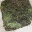 Given the huge economic incentives, corrosion prevention and protection is a major business. The advanced materials that are being developed and used in modern industries require increasingly sophisticated coatings for improved performance and durability. Take for example the case of microbially induced corrosion (MIC) - one of the lesser understood forms of corrosion where micro-organisms manifest metallic surfaces and induce substantial damage that often goes unnoticed until there is a loss in the component functionality. New research features graphene as a promising novel surface coating that can be used to minimize metallic corrosion under harsh microbial conditions.
Oct 13th, 2015
 The age of wearable electronics is upon us as witnessed by the fast growing array of smart watches, fitness bands and other advanced, next-generation health monitoring devices such as electronic stick-on tattoos. In order for these wearable sensor devices to become fully integrated into sophisticated monitoring systems, they require wireless interfaces to external communication devices such as smartphones. This requires far-field communication systems that, like the sensor systems, perform even under extreme deformations and during extended periods of normal daily activities.
Oct 9th, 2015
 Setting up or upgrading a lab to conduct state-of-the-art DNA nanotechnology is not an inexpensive undertaking. The hardware alone can easily set you back several hundreds of thousands of dollars. Analogous to the open-source software approach, increasingly instruments and specialized equipment designs are also developed as part of a growing open source scientific hardware (OSSH) movement. Adding to the list, a recent article presents three examples of open source/DIY technology with significantly reduced costs relative to commercial equipment.
Oct 7th, 2015
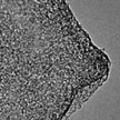 A carbon material with high electrical conductivity, high specific surface area, tunable pore structure, mechanically robust framework, and high chemical stability is an important requirement for advanced electrochemical energy storage. However, neither porous carbon or sp2 carbon can full meet these requirements yet. How to create a conductive carbon material with especially large pore volume, and hence large surface area, has therefore been a key focus in electrode research.
Oct 5th, 2015
 Researchers have demonstrated that perfect orbital angular momentum could be generated in optical nanostructures inspired by catenaries - the curve that a free-hanging chain assumes under its own weight. They used optical catenary-shaped structures to convert circularly polarized light to helically-phased beam carrying orbital angular momentum. Similar to the 'catenary of equal strength', the phase gradient of the optical catenary is equal everywhere, which is a direct result of its special geometric shape.
Oct 2nd, 2015
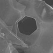 Synthesis of holey two-dimensional (2D) nanosheets with defined hole morphology and hole edge structures remains a great challenge for graphene. It is also an issue for other 2D nanomaterials, such as hexagonal boron nitride (h-BN) and molybdenum disulfide. In new work, researchers have reported a facile, controllable, and scalable method to carve geometrically defined pit/hole shapes and edges on h-BN basal plane surfaces via oxidative etching in air using silver nanoparticles as catalysts.
Oct 1st, 2015
 The development of nanoscale devices and applications requires ultra-sensitive sensing systems that can offer not only atomic resolution imaging but also sub nanometer scale displacement detection, zeptogram level mass sensing, or single bio-molecular sensing. Researchers have now developed a novel sensor that addresses some of the shortcomings that have plagued existing optical scanning systems , namely size, complexity, and cost. This sensing technology is completely electrical and capable of sensing very small displacement as low as in the femtometer range.
Sep 30th, 2015
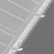
 To overcome the pixel size limitation of existing digital image sensors, both new materials with enormous photoelectric properties and novel device architectures are required. In new work, researchers are now reporting ultra-high resolution nanorod digital image sensor (NDIS) which is fabricated by sandwiching vertically aligned zinc oxide nanorod arrays between orthogonal top and bottom nanostripe electrodes. The most important application of the NDIS is as a next-generation digital image sensor with ultra-high resolution, well beyond the limit of existing techniques.
Sep 29th, 2015
 Subscribe to our Nanotechnology Spotlight feed