Showing Spotlights 113 - 120 of 154 in category All (newest first):
 Extracellular signaling molecules are the language that cells use to communicate with each other. These molecules transfer information not only via their chemical compositions but also through the way they are distributed in space and time throughout the cellular environment. With the development of nanosensing techniques, scientists are trying to to eavesdrop on the cellular whisper and they getting closer to deciphering extracellular signaling - an important task in understanding how cells organize themselves, for instance during organ development or immune responses. Now, researchers have reported a novel sensing technique to interrogate extracellular signaling at the subcellular level. They developed a nanoplasmonic resonator array to enhance fluorescent immunoassay signals up to more than one hundred times to enable the first time submicrometer resolution quantitative mapping of endogenous cytokine secretion from an individual cell in nanoscale close to the cell.
Aug 15th, 2011
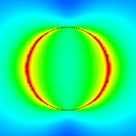
 Exotic artificial composite materials called metamaterials can be engineered with certain electromagnetic properties that allows them to act as invisibility cloaks. These materials bend all light or other electromagnetic waves around an object hidden inside a metamaterial cloak, to emerge on the other side as if they had passed through an empty volume of space. Researchers have already been experimenting with cloaking devices for various, usually longer wavelengths such as microwave or infrared waves. Recently, even graphene has been added to the family of cloaking materials. Now, for the first time, a team of scientists at UC Berkeley have devised an invisibility cloak material that hides objects from detection using light that is visible to humans.
Aug 3rd, 2011
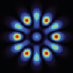
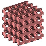 Photonic crystals are used to guide and localize light for all-optical processing of signals/information; to engineer dispersion and slow light; to harvest light (collect and redirect); and thresholdless lasing, that can be engineered by setting spectral ranges where light can be emitted. so far, there have been no demonstrations of full photonic bandgap at visible wavelengths - i.e., that at a certain visible range (between 400 nm to 780 nm) determined by the 3D photonic crystal structure, the light is rejected (reflected) at all angles of incidence. Researchers have now used a 3D nano-sculpturing process to fabricate 3D photonic crystal. The great potential of these 3D photonic crystal lies in the possibility to control light on a sub-wavelength scale.
Mar 23rd, 2011
 No matter how precise nanosensors and -probes become, bridging the huge gap between nanoscale dimensions and macroscale structures (e.g., wafer size) has been a tremendous challenge for researchers. Researchers in the U.S. have demonstrated a generalized hybrid nanofabrication concept that combines both top-down (deep-UV lithography) and bottom-up (controlled lateral epitaxial growth and atomic layer deposition) fabrication techniques. This unique methodology allows the development of reproducible nanostructured platforms that contain controlled sub-10 nm gaps between plasmonic nanostructures over an entire wafer, i.e. a 6-12 inch area. This approach opens new horizons to more widespread applications in chemical sensing and biomedical diagnostics.
Mar 2nd, 2011
 Silicon and III-V semiconductors are the respective foundations of modern electronics and photonics. Integrating these materials is essential for achieving new optoelectronic functionality and faster computer architecture. However, lattice mismatch and high III-V growth temperatures have prevented such integration thus far. Most importantly, in order to be able to take advantage of today's massive silicon infrastructure, integration must be compatible with current complementary metal-oxide-semiconductor (CMOS) infrastructure and process flows. Researchers at UC Berkeley have overcome these obstacles by developing a way to grow III-V nanolasers on silicon, demonstrating the potency of bottom-up nano-optoelectronic integration.
Feb 22nd, 2011
 One of the many fascinating concepts in nanotechnology is the vision of molecular electronics where researchers are investigating nanostructured materials to build electronics from individual molecules. If realized, the shift in size from even the most densely packed computer chip today would be staggering. Molecular electronics aims at the fundamental understanding of charge transport through molecules and is motivated by the vision of molecular circuits to enable miniscule, powerful and energy efficient computers. A research team in Germany has now demonstrated that rigidly wired molecules can emit light under voltage bias. This result is important for fundamental science but it also adds to the molecular electronics vision an optoelectronic component, i.e. the development of optoelectronic components on the basis of single molecules.
Nov 29th, 2010
 Aberrations in optical systems, which leads to blurring of the image, and their elimination using adaptive optics have been studied in astronomical research for quite a long time. Aberrations occur when light from one point of an object after transmission through the optical system does not converge into a single point. The complicated part in correcting this error usually lies in identifying the aberrations that need to be eliminated from the system. With the emergence of nanoscale applications, aberrations in modern microscopy have become a severe limitation on the optimal performance in imaging, nanosurgery, nanofabrication and micromanipulation, just to name a few. Researchers have now demonstrated a powerful method for aberration correction with a simple implementation that typically requires minimal changes in the particular geometry.
May 25th, 2010
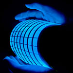 OLEDs - organic light-emitting diodes - are full of promise for a range of practical applications. OLED technology is based on the phenomenon that certain organic materials emit light when fed by an electric current and it is already used in small electronic device displays in mobile phones, MP3 players, digital cameras, and also some TV screens. With more efficient and cheaper OLED technologies it will possible to make ultra flat, very bright and power-saving OLED televisions, windows that could be used as light source at night, and large-scale organic solar cells. In contrast to regular LEDs, the emissive electroluminescent layer of an OLED consists of a thin-film of organic compounds. Exciton quenching and photon loss processes still limit OLED efficiency and brightness. Organic light-emitting transistors (OLETs) are alternative, planar light sources combining, in the same architecture, the switching mechanism of a thin-film transistor and an electroluminescent device. Thus, OLETs could open a new era in organic optoelectronics and serve as test beds to address general fundamental optoelectronic and photonic issues.
May 6th, 2010
 Subscribe to our Nanotechnology Spotlight feed