Showing Spotlights 121 - 128 of 154 in category All (newest first):
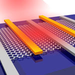 Silicon has dominated solid-state electronics for more than four decades but now a variety of other materials are being explored in photonic devices to expand the wavelength range of operation and to improve performance. Graphene is such a material - although most research on graphene so far has focused mainly on electronics. IBM researchers have now shown that graphene-based devices can be used in optical communications. Introducing this new material system into photonics could have a significant impact on mainstream optical applications. By using graphene, researchers make use of the internal electric field that exists at the interface of graphene and metal. Through a sophisticated combination of palladium and titanium electrodes they created a photodetector that does not rely on external current.
Apr 7th, 2010
 Spectrometers are used in materials analysis by measuring the absorption of light by a surface or chemical substance. These instruments measure properties of light over a specific portion of the electromagnetic spectrum. In conventional spectrometers, a diffraction grating splits the light source into several beams with different propagation directions according to the wavelength of the light. Thus, to achieve sufficient spatial separation for intensity measurements at a small slit, a long light path - i.e., a large instrument - is required. However, for lab-on-a-chip applications, the spectrometer must be integrated into a sub-centimeter scale device to produce a stand-alone platform. To achieve this, researchers at the Korea Advanced Institute of Science and Technology (KAIST) propose a new paradigm in which the spectrometer is based on an array of photonic crystals with different bandgaps.
Mar 8th, 2010
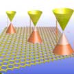 A group of researchers from Singapore, led by Professor Dingyuan Tang from Nanyang Technological University and Professor Kian Ping Loh from National University of Singapore, have reported the first breakthrough in using few-layer graphene as a saturable absorber for the mode locking of lasers. Despite its prominent mechanical and electrical properties, graphene's optical response has previously been considered to be weak and featureless, so the main interests of the research community are centered on its electronics properties. But now, Tang and Loh demonstrate that graphene can be used for telecommunications applications and that its weak and universal optical response might be turned into advantages for ultrafast photonics applications.
Jan 6th, 2010
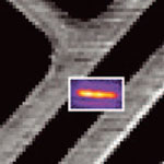
 Single molecule detection requires tools that have the detection sensitivity at the scale of single molecules. This could mean a spatial resolution requirement of only a few nanometers especially if the precise location of the molecule needs to be mapped. Researchers have already developed spectroscopic techniques capable of physical and chemical mapping on a nanometer scale. Researchers in Italy have now reported the design, fabrication and application of a photonic-plasmonic device that is fully compatible with atomic force microscopy and Raman spectroscopy - an approach that is novel in both scientific and technological aspects. The device consists of a two-dimensional dielectric photonic crystal cavity patterned on an AFM cantilever, together with a tapered silver waveguide placed at the center of the cavity.
Nov 24th, 2009
 Surface-plasmon resonance is a quantum-electromagnetic phenomenon arising from the interaction of light with free electrons at the planar interface of a metal and a (nonconducting) dielectric material. This resonance arises when the energy carried by photons in the dielectric material is transferred to collective excitations (called plasmons) of free electrons in the metal at that interface. As the free electrons in the metal are coupled to the photons in the polarizable dielectric material, the quantum is called a surface plasmon-polariton (SPP). Typically, a SPP wave is launched on a metal-dielectric interface at one particular frequency. That wave has a certain polarization state. Researchers have now shown theoretically and experimentally that by modifying the dielectric material, novel surface-plasmon-polariton wave behavior can be created with the result that the same interface can independently guide more than one SPP wave.
Oct 12th, 2009
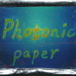 Photonic crystals are very suitable for fabricating sensor devices because the optical signals of these responsive materials are tightly coupled with various external stimuli and modulations. They could also play a significant role on the way to all-optical devices in communication and information technology - they form a basis material for the future realization of optical components and circuits, and maybe even complex optical circuits or optical computers. One application area that has seen a lot of activity recently is photonic paper and ink. One advantage of photonic papers and displays is that they are brilliant and free of glare in sunlight, which are superior to the characteristics of other emissive display technologies for outdoor usage such as advertising billboards. Another advantage is that, for recording purposes, the structural colors of photonic paper are usually more durable than traditional pigments and dyes. However, there are still a number of issues and problems that prevent the practical applications of the photonic crystal based materials. Researchers in California have now addressed some of them by reporting a new type of rewritable photonic paper on which a durable ink mark can be written or erased by introducing or removing a hygroscopic salt in the surface layer of the paper.
Aug 17th, 2009
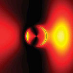
 The development of electron-beam lithography, focused ion beam milling, and other nanofabrication techniques has provided researchers with great freedom to pattern metallic structures at the nanoscale. This has fueled the design and implementation of new ultracompact photonic devices based on the plasmonic behavior of metals. Plasmonics is an emerging field of nanophotonics that relies on hybrid light-charge density waves on metal-dielectric interfaces and holds the promise for control of light at dimensions much below the free-space wavelength of light. Lenses have always been an important component for controlling light in optical systems. The focusing capability of conventional, dielectric-based microlenses however deteriorates as their physical dimensions are reduced toward a single-wavelength scale. That's why scientists have begun exploring alternative approaches to refractive lensing. While nano-patterning of optically thick metallic films was theoretically proposed as an alternative to refractive lensing, scientists at Stanford University have now reported the first experimental demonstration of far-field lensing using a plasmonic slit array.
Dec 19th, 2008
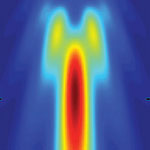
 Carbon nanotubes are considered a promising material system not only for nanoelectronics but also for nanophotonics - the manipulation and emission of light using nanoscale materials and devices. By trying to understand the electrical properties of carbon nanotubes (CNTs) through their light emission, scientists are paving the way for CNTs' integration in optical applications. Embedding spatially isolated CNTs into an optical microcavity is a promising means of controlling and improving their radiative properties. The control of these CNT properties, including emission wavelength, spectral width, emission direction and radiative yield through optical confinement, opens the door for their use in integrated nanophotonic circuits. Cavity controlled nanotube emitters could potentially find use in quantum optics, quantum communication, and integrated nanophotonic circuits and may ultimately lead to low threshold on-chip nanolasers.
Sep 9th, 2008
 Subscribe to our Nanotechnology Spotlight feed