Showing Spotlights 129 - 136 of 155 in category All (newest first):
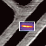 Carbon nanotubes are considered a promising material system not only for nanoelectronics but also for nanophotonics - the manipulation and emission of light using nanoscale materials and devices. By trying to understand the electrical properties of carbon nanotubes (CNTs) through their light emission, scientists are paving the way for CNTs' integration in optical applications. Embedding spatially isolated CNTs into an optical microcavity is a promising means of controlling and improving their radiative properties. The control of these CNT properties, including emission wavelength, spectral width, emission direction and radiative yield through optical confinement, opens the door for their use in integrated nanophotonic circuits. Cavity controlled nanotube emitters could potentially find use in quantum optics, quantum communication, and integrated nanophotonic circuits and may ultimately lead to low threshold on-chip nanolasers.
Sep 9th, 2008
 Photonic crystals are similar to semiconductors, only that the electrons are replaced by photons (i.e. light). By creating periodic structures out of materials with contrast in their dielectric constants, it becomes possible to guide the flow of light through the photonic crystals in a way similar to how electrons are directed through doped regions of semiconductors. The photonic band gap (that forbids propagation of a certain frequency range of light) gives rise to distinct optical phenomena and enables one to control light with amazing facility and produce effects that are impossible with conventional optics. A prominent example of a photonic crystal is the naturally occurring gemstone opal. The problem with artificial opals, which limits their applications, is that they lack in pattern variety and their fabrication requires very expensive equipment and sophisticated processes. In contrast, natural photonic crystals have various patterns that are quite promising structural matrices for creating novel optical devices. One example are peacock feathers, whose iridescent colors are derived from the 2D photonic crystals structure inside the cortex.
Aug 15th, 2008
 Optical imaging of materials is full with rich physical, chemical and biological information about the sample, because the optical energies in the visible range coincide with the atomic and molecular transition energies of many materials. Apart from the topographical information, the optical image therefore contains information about intrinsic properties of a material. However, the wave nature of light prevents the light to focus in a volume smaller than half of the wavelength, which is about 200-300 nm for visible light. Therefore, it is almost impossible to image nanomaterials, which could be a few nanometers in size, using optical imaging process. A typical lens made of, for example glass, will not be sufficient to image a nanomaterial. In work that gives rise to a new concept of a lens for optical imaging, scientists in Japan have proposed a lens made of silver nanorods, rather than a curved glass surface. This metallic nanolens is capable of manipulating light in such a way that an optical image of nanoscale objects can be obtained in the visible range.
Jun 17th, 2008
 Light-emitting nanostructures are widely used for optical, photonic, chemical, and biological devices. For example, fluorescent nanoparticles are useful for biological assays and as tumor markers, chemical sensors, and organic lasers, whereas one-dimensional luminescent nanowires are exploited for novel nanoscale photonic devices such as nano-lasers and nanowire scanning microscopy. While several methods to prepare organic, inorganic, and polymeric light-emitting nanostructures have been developed, the fabrication of luminescent nanoarchitectures with a tailored morphology and pattern is still challenging. Researchers in Korea have discovered that non-luminescent polystyrene can be converted into a luminescent organic material whose emitting color can be tuned from deep blue to white by electron irradiation. They demonstrated that luminescent nanopatterns are readily fabricated only by irradiating an electron beam to the selected regions of polystyrene. In addition, the top-down irradiation approach in conjunction with self-assembled polystyrene nanostructures allows fabrication of diverse and complex luminescent nanoarchitectures.
Jun 12th, 2008
 A key challenge in nano-optics is to bring light to and collect light from nano-scale systems. In conventional electronics, the interconnect between locally stored and radiated signals, for example radio broadcasts, is formed by antennas. For an antenna to work at the wavelength of light it needs to be greatly scaled down, to the nanoscale. Antennas play a key role in our modern wireless society. The electromagnetic waves sent and received by antennas are the messages that enable communication between electronics. Antennas with a wide variety of sizes make it possible for us receive radio broadcasts, watch television and talk to others on a mobile phone. For an effective communication, the antenna needs to direct signals towards their intended target and, vice versa, collect signals from a desired source. Now, researchers have shown that the concept of an antenna is equally well applied to direct the visible light sent out by a single molecule. For an antenna to work with visible light, it needs to be millions of times smaller than a conventional antenna. In this case, it is only 80 nanometer long. By placing the antenna near an individual molecule the light from that molecule is re-directed; the molecular message can be steered to a desired target, making efficient communication possible.
Mar 27th, 2008
 The success of the computer and communications industry is mainly due to the possibility of a large volume and low cost production output: silicon wafers containing myriad micro and nano structures are at the basis of Complementary Metal Oxide Semiconductor (CMOS) technology. A challenge is the realization of spatially ordered nanostructures in silicon that have many interesting applications like photonic crystals to mod the flow of light, chemical sensors, devices to alter the wetting of liquids on a surface, and as capacitors in high-frequency electronics used in mobile phones. The incorporation of such structures on existing silicon chips is greatly desired, and adapting conventional semiconductor nanofabrication to that end is widely pursued. Just a few days ago we wrote about the general aspects and challenges of silicon photonics and today we are taking a look at a specific fabrication challenge. The challenge for researchers is to to obtain photonic crystals with stop bands in the telecommunication wavelength regions, i.e.1330 nm and 1550 nm. To do that, the diameter of these pores must be smaller than 500 nm. The pore to pore distances, also referred to as pitch or interpore distance, must be well below 1 micrometer. Furthermore the depth to diameter aspect ratio of the pores must be as high as possible to obtain photonic crystals with large enough volumes. Researchers in The Netherlands now have demonstrated a method to etch arrays of nanopores in silicon with record depth-to-diameter ratios. These structures are suitable for nanophotonics and were made completely with CMOS compatible technologies, making integration of photonic structures in silicon chips feasible.
Mar 26th, 2008
 In its everlasting quest to deliver more data faster and on smaller components, the silicon industry is moving full steam ahead towards its final frontiers of size, device integration and complexity. We have covered this issue numerous times in previous Spotlights. As the physical limitations of metallic interconnects begin to threaten the semiconductor industry's future, one group of researchers and companies is betting heavily on advances in photonics that will lead to combining existing silicon infrastructure with optical communications technology, and a merger of electronics and photonics into one integrated dual-functional device. Today, silicon underpins nearly all microelectronics but the end of the road for this technology has clearly come into view. Photonics is the technology of signal processing, transmission and detection where the signal is carried by photons (light) and it is already heavily used in photonic devices such as lasers, waveguides or optical fibers. Optical technology has always suffered from its reputation for being an expensive solution, due to its use of exotic materials and expensive manufacturing processes. This prompted research into using more common materials, such as silicon, for the fabrication of photonic components, hence the name silicon photonics. Although fiber-optic communication is a well-established technology for information transmission, the challenge for silicon photonics is to manufacture low-cost information processing components. Rather than building an entirely new industrial infrastructure from scratch, the goal here is to to develop silicon photonic devices manufactured using standard CMOS techniques. A recent review paper takes a look at the state of silicon photonics and identifies the challenges that remain on the path to commercialization.
Mar 14th, 2008
 Shorter-wavelength surface-emitting laser sources are important for a variety of fields including photonics, information processing and biology. Researchers in Japan were successful in developing a current-driven blue-violet photonic crystal surface-emitting laser. They developed a fabrication method, named 'air holes retained over growth', in order to construct a two-dimensional gallium nitride/air photonic crystal structure. The resulting periodic structure has a photonic crystal band-edge effect sufficient for the successful operation of a current-injection surface-emitting laser. This represents an important step in the development of laser sources - from both a scientific and engineering point of view - that could be focused to a size much less than the wavelength and be integrated two-dimensionally at such short wavelengths.
Jan 2nd, 2008
 Subscribe to our Nanotechnology Spotlight feed