Showing Spotlights 169 - 176 of 330 in category All (newest first):
 Sodium-ion batteries (SIBs) represent an attractive alternative to lithium-ion batteries, owing to the fact that sodium resources are practically inexhaustible and evenly distributed around the world while the ion insertion chemistry is largely identical to that of lithium. Researchers have now rationally designed and fabricated a sodium ion full battery where both of the cathode and anode materials possessed very unique two-dimensional nanostructured architecture. The 2D nanostructured architecture results in excellent rate capability and stable cycling performance.
Aug 17th, 2016
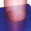 Graphene, one of the most exciting two-dimensional materials, has shown extraordinary optical properties due to strong surface plasmon polaritons supported by graphene nanostructure. Graphene metasurfaces show plasmonic resonance bands that can be tuned from mid-infrared to terahertz regime. These plasmonic devices can be used for biosensing, spectroscopy, light modulation and communication applications. Researchers now demonstrate for the first time an effective method to pattern large area graphene into moire metasurfaces with gradient nanostructures having multiband resonance peaks in mid infrared range.
Aug 16th, 2016
 Researchers have demonstrated that the coupling of pristine graphene sheets on practically any polymer surface can be accomplished in mild reaction conditions and in aqueous medium. The method leaves intact the 2D planar structure of graphene preserving its original features. This novel hybrid construct enables in vivo photoacoustic signal enhancement and is a very promising step forward for an implementation of photoacoustic imaging, a powerful preclinical diagnostic tool.
Jun 30th, 2016
 First there was graphene, an atomically thin film of carbon atoms with record-crushing properties. Then thousands of other atomically thin materials entered the scene which can be layered to create new hybrid supermaterials - so called van der Waals heterostructures. Until now, only a few leading groups have been able assemble these materials with sufficiently high quality. With the 'hot pickup' stacking method, researchers aim to make atomic scale nano-assembly faster and easier than ever before.
Jun 16th, 2016
 Inspired by the multiple water purification mechanisms of water hyacinth, a group of researchers has combined different decontamination techniques - adsorption, photocatalytic degradation, distillation - into a single paper-based composite system for water purification by using solar light as the clean energy input. Compared with water treatment with a single mechanism, the multifunctional composite reported in this work could significantly enhance the clean water generation efficiency and maximize the use of the broad-spectrum solar light in a facile and effective way.
Jun 14th, 2016
 Using multilayer graphene as an electrically reconfigurable optical medium, researchers have demonstrated an optoelectronic framework compatible with conventional printing paper. The device consist of two multilayer graphene layers transfer-printed on both sides of the paper. In this configuration, multilayer graphene simultaneously operates as the electrically reconfigurable optical medium and electrically conductive electrodes. In addition, the paper substrate yields a flexible and foldable mechanical support for the graphene layers and it holds the electrolyte in the network of hydrophilic cellulose fibers.
Jun 8th, 2016
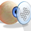 The latest example of a graphene-based wireless sensor that could make 24-hour healthcare easier to achieve by enabling wireless monitoring of various biomedical events in order to gain a more comprehensive assessment of the wearer's healthcare status. This novel device, which detects chemical/molecular agents and lengths of exposure, can be used as lightweight and transparent wearable or bio-implantable electronic sensor. It may provide an inexpensive way to detect in real-time the biomedical of interest.
Jun 6th, 2016
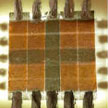
 High-temperature heaters, such as furnaces, are widely used in chemical reactions, materials synthesis and device processing. The limitations of these heating devices often are their bulky size, weight, low maximum heating temperatures and slow ramp rates. To overcome these limitations, and to provide a heating element with a high temperature range to the target object in a micro- and nanoscale environment, researchers have developed a 3D-printable high-temperature, high-rate heater that can be applied to a wide range of nanomanufacturing when precise temperature control in time, placement, and the ramping rate is important.
May 19th, 2016
 Subscribe to our Nanotechnology Spotlight feed