Showing Spotlights 193 - 200 of 252 in category All (newest first):
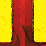 Chip structures already have reached nanoscale dimensions but as they continue to shrink below the 20 nanometer mark, ever more complex challenges arise and scaling appears not to be economically feasible any more. And below 10 nm, the fundamental physical limits of CMOS technology will be reached.
One promising material that could enable the chip industry to move beyond the current CMOS technology is graphene, a monolayer sheet of carbon. Notwithstanding the intense research interest, large scale production of single layer graphene remains a significant challenge. Researchers at Cornell University have now reported a new technique for producing large scale single layer graphene sheets and fabricating transistor arrays with uniform electrical properties directly on the device substrate.
Chip structures already have reached nanoscale dimensions but as they continue to shrink below the 20 nanometer mark, ever more complex challenges arise and scaling appears not to be economically feasible any more. And below 10 nm, the fundamental physical limits of CMOS technology will be reached.
One promising material that could enable the chip industry to move beyond the current CMOS technology is graphene, a monolayer sheet of carbon. Notwithstanding the intense research interest, large scale production of single layer graphene remains a significant challenge. Researchers at Cornell University have now reported a new technique for producing large scale single layer graphene sheets and fabricating transistor arrays with uniform electrical properties directly on the device substrate.
Dec 2nd, 2009
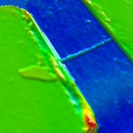
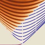 Graphene is an impressive condensed matter system that, to all appearances, never ceases to impress and challenge our entrenched intuitions regarding solid state systems. But graphene is a highly atypical electronic system in that it consists of nothing but a surface. Researchers at Boston University have found that local deformations in a graphene sheet can strongly influence electron flow across the system, causing suppression of conductance at low densities, and making electrons behave as if they were living in a nanoribbon or quantum dot. All this without cutting the graphene sheet, which opens the prospect towards a reversible and controllable transport gap in monolayer graphene via strain engineering.
Oct 6th, 2009
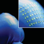 Imagine this: Chip-based credit cards and other smart cards on paper; intelligent sensors and electronics on doctors' surgical gloves; health monitors printed on T-shirts; diagnostic devices embedded in your baby's diapers; human machine interfaces on workers' leather gloves. These are just some of the systems that researchers envision today and that will become reality tomorrow thanks to research teams like John Rogers' group at the University of Illinois. Nanotechnology-enabled electronics of the future will be invisible, i.e. transparent, or flexible, or both. One of the areas Rogers' group focus on is creating materials and processes that will allow high-performance electronics that are flexible and stretchable. The group has now demonstrated examples of CMOS circuits on paper, fabric, leather and vinyl.
Oct 1st, 2009
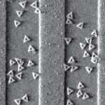 DNA origami, tiny shapes and patterns self-assembled from DNA, have been heralded as a potential breakthrough for the creation of nanoscale circuits and devices. One roadblock to their use has been that they are made in solution, and they stick randomly to surfaces - like a deck of playing cards thrown onto a floor. Random arrangements of DNA origami are not very useful; if they carry electronic circuits for example, they are difficult to find and 'wire-up' into larger circuits. A collaboration between Caltech and IBM research Almaden has found a way to position and orient DNA origami on surfaces by creating sticky patches in the shape of origami - as a demonstration they positioned and aligned triangular DNA origami on triangular sticky patches. This success knocks down one of the major roadblocks for the use of DNA origami in computer nanotechnology.
Aug 18th, 2009
 The degree of mobility of a semiconductor, i.e. how well it conducts, is crucial to the effectiveness of nanoelectronic devices. Mobility determines the carrier velocity, and hence switching speed, in FETs. Researchers have determined that the theoretical mobility of an individual single-walled carbon nanotube is about 1000 times higher than any other known semiconductor. However, practical applications would require massive manufacturing of large scale nanoelectronic devices. Despite progress being made with integrating individual nanotubes in lab environments, many of today's nanomanufacturing techniques for nanoelectronic devices rely on the use of 'carbon nanotube network films' comprised of multiple carbon nanotubes. The major problem here is that the electronic properties of CNT network films are usually very poor. Researchers in South Korea have now developed a powerful strategy to solve these fundamental problems simply by controlling the connectivity of nanotube/nanowire networks.
Aug 4th, 2009
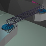 The fundamental issue of large-scale carbon nanotube (CNT) device fabrication remains the biggest challenge for effective commercialization of CNT-based nanoelectronic devices. For CNT electronics to become a reality requires manufacturing techniques to simultaneously and reproducibly fabricate a very large number of such devices on a single chip, each accessible individually for electronic transport. Conventional nanotube growth and device fabrication techniques using chemical vapor deposition or spin-casting are unable to achieve this, due to a lack of precise control over nanotube positioning and orientation. New work conducted at Tel Aviv University utilizes the CVD growth of CNTs over pillar-patterned silicon substrates to facilitate the formation of devices with taut and aligned CNTs grown exclusively at desired positions with built-in electrical contacts.
Jul 23rd, 2009
 The most promising applications of graphene are in electronics, detectors, and thermal management. The first graphene field-effect transistors have already been demonstrated. At the same time, for any transistor to be useful for analog communication or digital applications, the level of the electronic low-frequency noise has to be decreased to an acceptable level. Low frequency electronic noise dominates the noise spectrum to a frequency of about 100 kHz. Despite the fact that modern electronic devices such as cell phones and radars operate at a much higher carrier frequency, the low frequency noise is extremely important. Due to unavoidable non-linearities in devices and systems, the low frequency noise gets up-converted, and contributes to the phase noise of the system, thus limiting its performance. It is not possible to build a communication system or detector based on graphene devices until the noise spectral density is decreased to the level comparable with the conventional state-of-the-art transistors. Researchers at the University of California - Riverside have now reported the results of experimental investigation of the low-frequency noise in a double-gate graphene transistors.
Jul 14th, 2009
 The performance of devices like organic light emitting diodes (OLEDs), flexible solar cells, or plastic electronics is sensitive to moisture because water and oxygen molecules seep past the protective plastic layer over time and degrade the organic materials which form the core of these products. To protect these sensitive devices, barrier technologies have been developed that protect them from environmental degradation. State-of-the-art barrier materials employ metal oxide thin films, commonly from aluminum or silicon oxides, which provide excellent protection from atmospheric oxygen and water, but still suffer from problems. A new study demonstrates a nanocomposite material that can initiate self-healing upon the influx of water through pores and cracks by delivering titanium dioxide nanoparticles to the defective site, which ultimately slows the rate of moisture diffusion to the reactive electronic device.
Dec 9th, 2008
 Subscribe to our Nanotechnology Spotlight feed