Showing Spotlights 2113 - 2120 of 2781 in category All (newest first):
 Modern fuel cells have the potential to revolutionize transportation. Like battery-electric vehicles, fuel cell vehicles are propelled by electric motors. But while battery electric vehicles use electricity from an external source and store it in a battery, fuel cells onboard a vehicle are electrochemical devices that convert a fuel's chemical energy directly to electrical energy with high efficiency and without combustion. One of the leading fuel cell technologies developed, in particular for transportation applications, is the proton exchange membrane (PEM) fuel cell, also known as polymer electrolyte membrane fuel cells - both resulting in the same acronym PEMFC. These fuel cells are powered by the electrochemical oxidation reaction of hydrogen and by the electroreduction of the oxygen contained in air. Presently, platinum-based electrocatalysts are the most widely used in PEM fuel cell prototypes. However, this metal is expensive due to its limited supply and its price is highly volatile. This creates one of the major barriers preventing commercialization of PEMFCs - the lack of suitable materials to make them affordable. Nanotechnology provides solutions to this problem.
Oct 31st, 2008
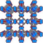 Crystalline nanoporous compounds have attracted the attention of scientists and materials engineers because of the interest in creating nanoscale spaces and the novel phenomena in them. Nanoporous materials find applications in many chemical processes such as separation and catalysis and are also heavily researched as storage materials, for instance in hydrogen fuel cells. Researchers still lack a complete understanding of the mechanism that leads to, and occurs during, crystal growth. Only once scientists achieve full control of properties such as composition, structure, size, morphology, and the presence and form of defects within the crystals can they fully exploit the benefits of crystalline nanoporous materials for the fabrication of novel materials. Researchers in the UK have now presented definitive real-time evidence of the crystal growth mechanism in what appears to be the first high-resolution observation of in-situ crystal growth of a crystalline nanoporous material monitored using atomic force microscopy (AFM).
Oct 30th, 2008
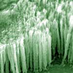 Nanostructured boron and boron-related compounds have attracted considerable scientific attention to exploit their potential use in high temperature electronics, thermoelectrics, and photovoltaics due to their unique chemical and physical properties, such as chemical inertness, hardness, and adjustable energy bandgap. Boron's theoretical tubular structures may even have higher electrical conductivity than carbon nanotubes (CNTs). So far, carbon nanotubes have been considered the most promising material for field emitters, for instance as electron emitters for field emission displays. Field emission results from the tunneling of electrons from a metal tip into vacuum, under application of a strong electric field. The small diameter and high aspect ratio of CNTs is very favorable for field emission. Due to the still existing difficulties of synthesizing CNTs with uniform chirality, a number of technical questions - such as stability, low melting point and uniformity of field emission - remain to be overcome. So scientists still looking to find other ideal candidates. New experiments conducted by scientists in China suggest that boron nanowires might fit the bill.
Oct 29th, 2008
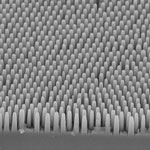 Antireflection coatings have become one of the key issues for mass production of silicon solar cells. Silicon solar cells are the most common solar cells on the market today. They are constructed with layers of n-type silicon having many electrons and p-type silicon having many electron holes. When hit by sunlight, an equal number of electrons and electron holes are generated at the interface between the two silicon layers and, as the electrons migrate from the n-type silicon to the p-type silicon, an electric flow is generated. One of the problems with silicon solar cells is the high refractive index of silicon, which causes more than 30% of incident light to be reflected back from the surface of the silicon crystals. Solar cell manufacturers have therefore developed various kinds of antireflection coatings (ARCs) to reduce the unwanted reflective losses. Currently, quarter-wavelength silicon nitride thin films deposited by plasma-enhanced chemical vapor deposition (PECVD) are the industrial standard for ARCs on crystalline silicon substrates. Unfortunately, current top-down lithographic techniques for creating subwavelength silicon gratings, such as electron-beam lithography, nanoimprint lithography, and interference lithography, require sophisticated equipment and are expensive to implement, thus contributing to the still high costs of this type of solar cells. Borrowing from Mother Nature's millions of years old design book, researchers have now come up with a nanotechnology antireflection coating inspired by the eyes of moths.
Oct 28th, 2008
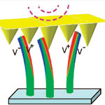 A major issue for using self-contained nanodevices, for instance as implantable nanosensors or environmental monitoring devices, is the question of how to power these tiny machines with an independent power source. Options include nanobatteries and nanogenerators that harvest energy from their environment. By converting mechanical energy from body movement, engine vibrations, or water or air flow into electricity, these nanoscale power plants could make possible a new class of self-powered medical devices, sensors and portable electronics. Probably the leading team that is driving forward the work on nanogenerators for converting mechanical energy into electricity is Zhong Lin Wang's group at Georgia Tech. Wang's team has now designed and demonstrated an innovative approach to fabricating a nanogenerator by integrating nanowires and pyramid-shaped nanobrushes into a multilayer power generator. By demonstrating an effective way for raising the output current, voltage and power, this work provides the technological platform for scaling up the performance of nanogenerators to a level that some day might be able to independently power devices like pacemakers or iPods.
Oct 27th, 2008
 The method that has been traditionally used in binary information storage is by making a distinction between storage (designated as 1) and non-storage (designated as 0). In reality, each imprint (or non-imprint) can store either 1 or 0. Thus the sequence and the numbers of 1 and 0 define everything with respect to the amount of information that can be stored and retrieved at the hardware level, no matter how sophisticated the overlaying software routines are. Ever since computers were developed, information storage has adhered to the eight-bit system. No matter how sophisticated information storage technologies have become - exploiting magnetoresistance, developing optical storage media such as CDs, DVDs and blue-ray discs, or the development of holographic storage media - a bit is always represented by manipulating a single feature, i.e., a transition or non-transition. Now, in contrast, consider the following: There are four colors, each of which could at least represent two or more bits; whereas in conventional methods only a single bit is available. In terms of color, this is somewhat similar to a black and white system that can support at most two kinds of transitions - 0 to 1 and 1 to 0. On the other hand, in four-color coded systems there can be 16 such unique transitions.
Oct 23rd, 2008
 There is a general perception that nanotechnologies will have a significant impact on developing 'green' and 'clean' technologies with considerable environmental benefits - be it in areas ranging from water treatment to energy breakthroughs and hydrogen applications. As a matter of fact, renewable energy applications probably are the areas where nanotechnology will make its first large-scale commercial breakthroughs. Conflicting with this positive message is the growing body of research that raises questions about the potentially negative effects of engineered nanoparticles on human health and the environment. However, there is one area of nanotechnology that so far hasn't received the necessary attention: the actual processes of manufacturing nanomaterials and the environmental footprint they create, in absolute terms and in comparison with existing industrial manufacturing processes. Analogous to other industrial manufacturing processes, nanoproducts must proceed through various manufacturing stages to produce a material or device with nanoscale dimensions.
Oct 22nd, 2008
 Nanoscale membranes are of great interest to researchers not only for nanofiltration applications but also in areas such as flexible electronics, extremely sensitive sensors, nanomedical applications and biomolecular research. Many of these applications would require the nanomembranes to be arranged in three-dimensional structures such as tubes, helices, rings, or wrinkles. So far, the roll-up of ultra-thin layers was heavily limited in materials choice, in most cases involving epitaxial semiconductor layers. The fabrication often requires a selective underetching procedure to release the nanomembranes from their substrate, a process which not only removes the underlying sacrificial layer but also in many cases dissolves the nanomembrane material itself. A new approach developed by scientists in Germany and Hong Kong now allows controlled fabrication of pure metal and oxide tubes as well as many other material combinations. They describe a general method to produce well-defined micro- and nanotubes from thin solid films deposited by mass production tools.
Oct 21st, 2008
 Subscribe to our Nanotechnology Spotlight feed