Showing Spotlights 2137 - 2144 of 2779 in category All (newest first):
 The concept of a 'machine' - a mechanical or electrical device that transmits or modifies energy to perform a certain task - can be extended to the nano-world. On the nanoscale, the nanomachine components would be atomic or molecular structures each designed to perform a specific task which, all taken together, would result in a complex function. However, these nanomachines can not be built by just further miniaturizing machine blueprints from the macro-world. Functional nanomachinery will need to take into account the quantum effects that dominate the behavior of matter at the nanoscale, affecting the optical, electrical and magnetic behavior of materials. Scientists in The Netherlands are now reporting how an atomic scale mechanical device consisting of two moving parts, each composed of only two atoms can be controlled by an external electrical signal, while being stable and providing a variety of functional modes. They jokingly refer to it as playing atomic pinball, since the two moving parts resemble the flippers in a pinball machine - unfortunately they haven't got a ball yet to play with.
Sep 23rd, 2008
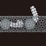 The processes by which molecules pass through pores in thin films and biological membranes are essential for understanding various physical, chemical and biological phenomena. For instance, the fundamental behavior of molecules in porous solids and their transfer through cell membranes necessarily involves a process of molecules passing through pores - knowledge that, for instance, is crucial for the development of nanotechnology-based hydrogen storage materials for fuel tanks. So far, research methods have been based on studying the statistical average of the behavior of groups of molecules; there were no experimental approaches that examined the interaction of a single molecule with a pore. There has been a lack of experimental methods that can obtain information on the structure and orientation of the molecules as they pass through a pore, and their interactions with the pore during passage. Researchers in Japan have now succeeded for the first time in observing a long chain of a fullerene-labeled hydrocarbon passing through a nanometer-size pore in the wall of a carbon nanotube as if it were alive.
Sep 22nd, 2008
 Travel through wormholes, time machines and hovering landspeeders are the stuff of science fiction novels. Nevertheless, scientists have suggested that the quantum mechanics of something called the Casimir effect can be used to produce a locally mass-negative region of space-time, a phenomenon that theoretically could be used to stabilize a wormhole to allow faster than light trave. For many years the Casimir effect was little more than a theoretical curiosity. With the advances in micro- and nanotechnology and the fact that the Casimir force affects nanoscale devices such as NEMS, research in detecting and manipulating this mysterious force has generated substantial interest. Now, the secretive DARPA, a research agency of the U.S. Department of Defense that often dabbles in far-out technologies - and that also brought us the Internet's predecessor ARPANET - is soliciting innovative research proposals in the area of Casimir Effect Enhancement.
Sep 19th, 2008
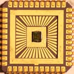 For nanoelectronics applications like single-electron devices to become practical, everyday items, they need to move from the highly individual and customized fabrication process typically found in laboratories to an automated, high-throughput and industrial-scale production environment. The reason this hasn't happened yet is that the various nanoscale pattern definition techniques used today - such as e-beam lithography, mechanically controllable break junctions, electromigration, electrodeposition, nanoscale oxidation, and scanning tunneling microscopy - generally are not suitable for large-scale parallel processing. The fabrication of single-electron devices requires nanoscale geometrical arrangement of device components, that is, source and drain electrodes and Coulomb islands. Developing methods to fabricate nanoscale devices in large numbers at a time has been one of the major efforts of the nanotechnology community. A new study now demonstrates that this can be done with complete parallel processing using CMOS-compatible processes and materials. Furthermore, these single-electron devices can operate at room temperature, an essential requirement for practical implementations.
Sep 18th, 2008
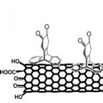 Pristine carbon nanotubes (CNTs) are insoluble in many liquids such as water, polymer resins, and most solvents. This means they are difficult to evenly disperse in a liquid matrix such as epoxies and other polymers, complicating efforts to utilize CNTs' outstanding physical properties in the manufacture of nanocomposite materials, as well as in other practical nanotechnology applications which require preparation of uniform mixtures of CNTs with many different organic, inorganic, and polymeric materials. To make nanotubes more easily dispersible in liquids, it is necessary to physically or chemically attach certain molecules, or functional groups, to their sidewalls without significantly changing the nanotubes' desirable properties. This process is called functionalization. Numerous nanotechnology research projects around the world are dedicated to developing various kinds of CNT-based electrochemical devices through the rational functionalization of CNTs.
Sep 17th, 2008
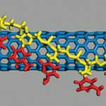 Current production methods for carbon nanotubes (CNTs) result in units with different diameter, length, chirality and electronic properties, all packed together in bundles, and often blended with some amount of amorphous carbon. These mixtures are of little practical use since many advanced applications, especially for nanoelectronics, are sensitively dependent on tube structures. Consequently, the separation of metallic and semiconducting CNTs is essential for future applications and studies. The tube diameter of semiconducting nanotubes is also important because the band gap depends on it. Separation of nanotubes according to desired properties is still proving to be a challenging task, especially single-walled carbon nanotube (SWCNT) sorting, because the composition and chemical properties of SWCNTs of different types are very similar, making conventional separation techniques inefficient. The separation techniques for SWCNTs explored to date rely on preferential electron transfer on metallic SWCNTs treated with diazonium salts, dielectrophoresis, enhanced chemical affinity of semiconducting SWCNTs with octadecylamine, and wrapping of SWCNTs with single-stranded DNA.
Sep 16th, 2008
 Complex technical and scientific issues means complex intellectual property issues. This especially is the case with nanotechnologies, which are not easy to classify. Patents are of critical importance for start-ups and smaller companies because they may help in negotiations over infringement of their patents during competitive posturing with larger corporations. There is also ample evidence that companies, start-ups, and universities are ascribing ever-greater value and importance to patents. Increasingly, they are willing to risk a larger part of their budgets to acquire and defend patents. A new book on bionanotechnology lists nine key considerations and strategies that bionanotechnology inventors must follow in order to adequately protect an invention even before a patent application is drafted or filed.
Sep 15th, 2008
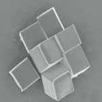 Using nanoparticles to combat cancer and a host of other diseases is an active area of research for many scientists. For decades, treating cancer has mostly involved injecting patients with toxic drugs. A practice, in which only a fraction of the drugs reach the intended target, killing healthy cells in the process and causing harmful side effects. Previous studies have shown that drug-carrying nanoparticles can accumulate in and attack tumors, in part because of their extremely small size, which helps allow them to pass through cell membranes. However, up until now, existing techniques have meant that targeting agents could only be delivered using spherical or granular shaped particles. Now, a team of scientists have demonstrated that nanoparticles designed with a specific shape, size and surface chemistry are taken up into cells and behave differently within cells depending on the characteristics of the particle.
Sep 11th, 2008
 Subscribe to our Nanotechnology Spotlight feed