Showing Spotlights 2345 - 2352 of 2784 in category All (newest first):
 Earlier this year, the Science Policy Council of the U.S. Environmental Protection EPA (EPA) issued the final version of its Nanotechnology White Paper. The purpose of this White Paper is to inform EPA management of the science issues and needs associated with nanotechnology, to support related EPA program office needs, and to communicate these nanotechnology science issues to stakeholders and the public. While this has been the publicly most visible EPA activity with regard to nanotechnology, it is less widely known that the EPA, since 2002, has been spending more than $25 million through its Science to Achieve Results (STAR) grants program for 86 projects on research into the environmental aspects of nanotechnology. The projects are broadly grouped into two main categories: 1) nanotechnology applications - examining beneficial uses - where the areas of research include green manufacturing, contamination remediation, sensors for environmental pollutants, and waste treatment; and 2) nanotechnology implications - examining the potentially adverse health effects to humans and the environment - where research is grouped into five categories: aerosol, exposure assessment, fate and transport, life-cycle analysis, and toxicity.
Nov 21st, 2007
 Tie a rock to the end of a piece of ribbon, then spin it over your head. It will be pulled taut as the rock circles about. Now, imagine a ribbon 62,000 miles long, anchored near the equator with a weight on the other end. The centrifugal force of the earth's rotation will make it behave the same way. You'll end up with not only the world's biggest nunchuck, but also a kind of elevator to outer space. A space elevator is one of those ideas from 1950s-style futurism that are so whacky they might just work. The single most difficult task in building the Space Elevator is achieving the required tether strength-to-weight ratio - in other words, developing a material that is both strong enough and light enough to support the 60,000 mile long tether. This material has become available in the form of carbon nanotubes (CNTs). The challenge ahead is to weave these raw CNTs into a useful form - a space worthy climbable ribbon. Assembling carbon nanotubes into commercially usable fibers is still one of the many challenges that nanotechnology researchers are faced with when trying to exploit the amazing properties of many nanomaterials. Apart from ambitious large-scale projects like the space elevator, CNT-based fibers will have many applications, from protective fabrics and coatings in military applications, higher performance materials for sports equipment to transparent conductive films and, eventually, as a replacement for copper wire in transmitting electrical power and signals. Researchers in the UK are making good progress in developing scalable fabrication techniques for high performance CNT fibers.
Nov 20th, 2007
 We have written Spotlight after Spotlight pointing out the numerous challenges that researchers are facing with regard to nanofabrication. Uncountable research papers have been written about the numerous methods available for synthesizing nanomaterials. What today is called 'nanofabrication' deals with the issues of fabricating complex and functional nano- and microstructures by integrating these synthesized nanomaterials. To complicate matters, many of these nanomaterials are fragile, either because they are composed of a limited number of atomic layers or because they are 'soft', i.e., of biological or molecular nature. This fragile nature of some materials creates a major headache: how to integrate them at an individual level into devices without altering their structure and, consequently, their properties during device fabrication. Currently, researchers use mainly e-beam lithography and, in some cases, focused ion beam to fabricate devices which incorporate nanostructures. These methods have been proven to be very useful, for example for investigations of carbon nanotubes. However, they can not be applied on fragile nanostructures, because they damage or contaminate the structures - this could result from exposure to high energy particle beams; the requirement for lift-off steps; exposure to chemicals, etc. Researchers have now shown that individual nanostructures can be integrated into functional devices using dynamic nanostenceling which allows the integration of individual nanostructures into devices using entirely scanning probe based methods and without exposure to damaging conditions, such as high-energy charged particles, heat, or resists.
Nov 19th, 2007
 The concept of e-noses - electronic devices which mimic the olfactory systems of mammals and insects - is very intriguing to researchers involved in building better, cheaper and smaller sensor devices. A better understanding of the reception, signal transduction and odor recognition mechanisms for mammals, combined with achievements in material science, microelectronics and computer science has led to significant advances in this area. Nevertheless, the olfactory system of even the simplest insects is so complex that it is still impossible to reproduce it at the current level of technology. For example, the biological receptors are regularly replaced during the life of mammals in a very reliable way so that the receptor array does not require to be recalibrated. The performance of existing artificial electronic nose devices is much more dependent on the sensor's aging and, especially, the sensor's replacement and frequently require a recalibration to account for change. Moreover, current electronic nose devices based on metal oxide semiconductors or conducting polymers that specifically identify gaseous odorants are typically large and expensive and thus not adequate for use in micro- or nano-arrays that could mimic the performance of the natural olfactory system. Nanotechnology is seen as a key in advancing e-nose devices to a level that will match the olfactory systems developed by nature. Nanowire chemiresistors are seen as critical elements in the future miniaturization of e-noses. It is now also believed that single crystal nanowires are most stable sensing elements what will result in extending of life-time of sensors and therefore the recalibration cycle. Last year we reported on a research effort Towards The Nanoscopic Electronic Nose. Scientists involved in this effort now report a second-generation, far more advanced e-nose system based on metal oxide nanowires.
Nov 16th, 2007
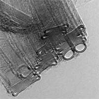
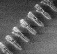
 A team of researchers have come up with an inexpensive way of making complex networks of carbon nanotubes that can be stamped onto circuit boards. They were able to create an inexpensive and relatively simple method for creating these predefined networks. The scientists arranged silicon pillars in the shape of the network they wanted and then coated the top of the pillars with silicon dioxide. The suspended single-walled carbon nanotubes adhered to the tops of pillars, growing taut and straight. A Raman spectroscopy (RS) laser not only assigned specific properties to each individual nanotube, it was also capable of destroying any unwanted nanotubes.
Nov 15th, 2007
 Slowly but surely the realization begins to sink in that there is no quick buck to be made for individual investors in nanotechnology companies (except for the people pushing investment advice of course). Existing public nanotechnology firms as a group have performed sub-standard (to put it politely); there isn't exactly a flood of nanotech IPOs on the horizon; and many product advances that have to do with nanotechnologies are made by large companies which either make these advances silently (witness the cosmetics industry) or tout them as major breakthroughs (like IBM's 'airgap' technology). In any case, all these nanotechnology-based materials are incremental improvements over existing materials - leading to better coatings, more efficient batteries and fuel cells, better performing materials, etc. - and not revolutionary devices. Of course, when we look back 10 years from now, there will have been one or two great performing nanotech stocks (I will tell you in 2017 who they are); but then there will be one or two great performing stocks in almost any other investment sector. Nevertheless, there are many start-ups and early stage companies out there - some might even make it to the IPO (initial public offering) stage or be bought by larger companies - and given the nature of the field, with its broad and multidisciplinary character, it certainly is helpful for the professional investor to be able to gauge the nanotechnology investment landscape from a technology perspective. A recent article describes a methodology to categorize different nanotechnologies into one of three types: passive, active, or hybrid nanotechnologies, each with different time horizons for expected commercial viability.
Nov 14th, 2007
 Fundamental nanotechnology research in laboratories advances rapidly, as witnessed by the hundreds of new research papers that get published every month. The big bottleneck in getting these new technologies from the lab translated into commercial products is the lack of suitable large-scale fabrication techniques. Almost all laboratory experiments involve elaborate set-ups and are quite tricky processes that require a lot of skill and expertise on part of the researchers. To a large degree, nanotechnology today is more an art than a basis for industrial technologies. Think about a 15th century monk spending 10 years painstakingly writing and painting a single bible - that's where nanotechnology is today; but where we need to get to is something that resembles modern high speed printing machines where you print thousands of books an hour. Take for instance nanowires. Researchers have used nanowires to create transistors like those used in memory devices and prototype sensors for gases or biomolecules. A common approach in the lab is to grow nanowires like blades of grass on a suitable substrate, mow them off and mix them in a fluid to transfer them to a test surface, using some method to give them a preferred orientation. When the carrier fluid dries, the nanowires are left behind like tumbled jackstraws. Using scanning probe microscopy or similar tools, researchers hunt around for a convenient, isolated nanowire to work on, or place electrical contacts without knowing the exact positions of the nanowires. It's not a technique suitable for mass production. However, researchers have now developed a technique that allows them to selectively grow nanowires on sapphire wafers in specific positions and orientations accurately enough to attach contacts and layer other circuit elements, all with conventional lithography techniques. This fabrication method requires a minimum number of steps and is compatible with today's microelectronics industry.
Nov 13th, 2007
 Some pundits writing about nanotechnology get carried away by their own hype and talk about self-assembly as if bottom-up fabrication technologies, where molecules get assembled into everyday products, are just around the corner. We took a swing at this in our Spotlight from a few days ago (Nanotechnology 'pencil sharpeners' add to researchers' nanofabrication toolbox). Today we bring you another example from the cold reality of the labs that makes clear how early stages this whole field of self-assembly really is. Today, when researchers - with both feet firmly on the ground - talk about self-assembly they mostly talk about template-assisted nanocrystal superlattices in the form of planar thin films. Bottomline is that even the controllable fabrication of highly ordered homogeneous nanostructures on surfaces remains a difficult challenge. And IBM's much touted 'self-assembling nanotechnology' (see: IBM applies self-assembling nanotechnology to conventional chip manufacturing) is nothing more than a patterning process that creates a film with trillions of holes around the on-chip wiring. Moving from a planar geometry of self-assembled nanoscale building blocks such as nanocrystals or nanotubes to a free-standing, three-dimensional multifunctional architecture is not a trivial undertaking. Researchers are just about to make the first steps to such multifunctional (still nanoscale) hierarchical architectures that both retain the properties of the nanocrystals and offer multifunctionality.
Nov 12th, 2007
 Subscribe to our Nanotechnology Spotlight feed