Showing Spotlights 2489 - 2496 of 2783 in category All (newest first):
 Nanowires have received a great deal of interest in recent years. As quasi one-dimensional systems they may overcome the fundamental difficulty in the electronic transport encountered when attempting to use quasi zero-dimensional structures (quantum dots) while still being able to take advantage of the effects related to quantum confinement. In a conventional semiconductor, electrons and holes typically stay in the same region after photoexcitation, which is very desirable for certain applications, light-emitting devices for instance. However, for a number of key renewable energy applications, including hydrogen generation via photoelectrochemical water splitting, dye-sensitized solar cells, and even regular solar cells, the efficient charge separation of the electron and hole after photoexcitation is instead highly preferred, although not readily available in the existing repertory of materials. In this context, researchers have explored the use of core-shell nanowires for such applications. However, for the material combinations that have been investigated, the energy alignments between the core and the shell are typically type I, and thus, the role of the shell is to either provide quantum confinement to both electrons and holes in the core or a protective cladding to the core to reduce sensitivity to the environment. Researchers at the National Renewable Energy Laboratory and Lawrence Berkeley National Laboratory designed a new class of core-shell semiconductor nanowires with strong type II band alignments. The photo-generated electron and hole in such nanowires are naturally separated in the core and shell, respectively, making them much more suitable for the solar energy applications than type I core-shell nanowires.
Apr 20th, 2007
 There seems to be an arms race going on among nanotechnology investment and consulting firms as to who can come up with the highest figure for the size of the "nanotechnology market". The current record stands at $2.95 trillion by 2015. The granddaddy of the trillion-dollar forecasts of course is the National Science Foundation's (NSF) "$1 trillion by 2015", which inevitably gets quoted in many articles, business plans and funding applications. The "nanotechnology market" as a unified market was first quantified by the NSF in its massive 280-pages report from March 2001. The problem with these forecasts is that they are based on a highly inflationary data collection and compilation methodology. The result is that the headline figures - $1 trillion!, $2 trillion!, $3 trillion! - are more reminiscent of supermarket tabloids than serious market research. Some would call it pure hype. This type of market size forecast leads to misguided expectations because few people read the entire report and in the end only the misleading trillion-dollar headline figure gets quoted out of context, even by people who should now better, and finally achieves a life by itself.
Apr 19th, 2007
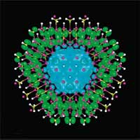
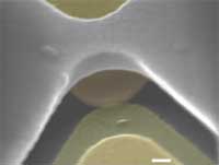
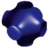 Self assembled structures from colloidal particles have many applications in biology, as chemical sensors and as photonic crystals. The control of shape and valency of the colloidal particle is very important since it will determine the 3D lattices of the assembled structure. There have been several prior effort to fabricating particles with complex shapes. Most particles with anisotropic shape are from the simple assembly of spheres or the modification of spherical particles. Interference lithography is one of the few techniques which can provide direct and systematic control over symmetry and volume fraction of the 3D structure. It involves the simple creation of interference patterns in a photoresist systems and subsequent pinch off of the parent structure through a drying process. Researchers at MIT have now presented a new facile and high-yield route for the fabrication of highly nonspherical complex multivalent nanoparticles. This technique exploits the ability of holographic interference lithography to control network topology. These research results could lay the groundwork for establishing and demonstrating control over particle shape in colloidal nanoparticles.
Apr 17th, 2007
 Nano-this and nano-that. These days it seems you need the prefix "nano" for products or applications if you want to be either very trendy or incredibly scary. This "nanotrend" has assumed "mega" proportions: Patent offices around the world are swamped with nanotechnology-related applications; investment advisors compile nanotechnology stock indices and predict a coming boom in nanotechnology stocks with misleading estimates floating around of a trillion-dollar industry within 10 years; pundits promise a new world with radically different medical procedures, manufacturing technologies and solutions to environmental problems; nano conferences and trade shows are thriving all over the world; scientific journals are awash in articles dealing with nanoscience discoveries and nano- technology breakthroughs. Nanotechnology has been plagued by a lot of hype, but cynicism and criticism have not been far behind. Science fiction writers exploit fears of nanorobots turning into killers; the media can run amok when news about potential health problems with nanoproducts surface (as happened last year with a product recall for a bathroom cleaner in Germany). Some see doomsday scenarios of molecular self-assembly turning the world into "grey goo." The emerging polarization of opinions on nanotechnology is reminiscent of controversies about genetically modified plants or nuclear energy. Vague promises of a better life are met by equally vague, generalized fears about a worse future. These debates have some aspects in common: the subject is complex and not easy to explain; there is no consensus on risks and benefits; scientists and corporations seem able to proceed unchecked, and it is unclear who is in control.
Apr 16th, 2007
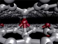 Research into the subject of radiation damage in graphite began in the early 1940s as a part of the development of nuclear weapons and nuclear power. Some designs of nuclear power reactors, such as the Chernobyl reactors, use graphite as moderator (the material which slows down the neutrons released from fission so that they cause more fission). The damage to the graphite moderators caused by radiation has been one of the major concerns of the nuclear power industry and radiation defects, i.e. structural irregularities, in graphite produced upon irradiation, their structure, properties and formation mechanisms, have been subject of intense research. Several years ago, defects in carbon materials became a hot topic again but now in the context of carbon layered nanostructures, such as multiwalled and bundled carbon nanotubes, which closely resemble graphite in their structure. The formation of irradiation-induced defects in graphite like layered carbon nanostructures, multiwalled and bundled carbon nanotubes, nanoonions, etc. changes their mechanical and electronic properties and may even trigger dramatic structural changes. While the terms "radiation damage" and "defect" are perceived negatively by people, the nanoengineering research community is trying to make use of defect structures for the deliberate modification of carbon nanomaterials, which can eventually be used in the manufacturing of nanoelectromechanical systems (NEMS). This process is sometimes called "defect-assisted engineering."
Apr 13th, 2007
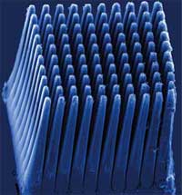 For computer chips, 'smaller and faster' just isn't good enough anymore. Power and heat have become the biggest issues for chip manufacturers and companies integrating these chips in everyday devices such as cell phones and laptops. The computing power of today's computer chips is provided mostly by operations switching at ever higher frequency. This physically induced power dissipation represents the limiting factor to a further increase of the capability of integrated circuits. Heat dissipation of the latest Intel processors has become a widely discussed issue. By the end of the decade, you might as well be feeling a rocket nozzle than touching a chip. And soon after 2010, computer chips could feel like the bubbly hot surface of the sun itself. As the electronics industry continues to churn out smaller and slimmer portable devices, manufacturers have been challenged to find new ways to combat the persistent problem of thermal management. New research suggests that the integration of carbon nanotubes (CNTs) as heat sinks into electronic devices might provide a solution to this problem.
Apr 12th, 2007
 Organic materials offer new electronic functionality not available in inorganic devices. Promising examples of novel characteristics in organic devices range from the memory effects observed in monolayers and polymer films to negative differential resistance devices. However, the integration of organic compounds within nanoscale electronic circuitry poses considerable challenges for materials physics and chemistry, and a detailed understanding of the conduction mechanisms, switching and memory is still lacking. With increasing research into very different material systems such as oxides, solid-state electrolytes, phase-change memory materials, it is becoming clear that electronic switching on the smallest length scale cannot be purely electronic phenomena. Rather, a motion of heavier constituents has to be involved that will in turn change the electronic properties. New work conducted at Bell Labs demonstrates the success of such a line of thought in molecular systems. The Bell scientists demonstrated a novel approach to creating and chemically modifying conducting electronic states in nanoscale molecular devices.
Apr 11th, 2007
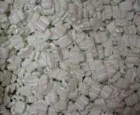 Polystyrene (PS), also known under its trademark name styrofoam, is found in your home, office, local grocery, fast food outlet and in the cafeteria. It comes in many shapes and forms, from foam egg cartons and meat trays, plates and salad boxes, from coffee cups and utensils to CD jewel boxes, and from produce trays to those foam peanuts used in packing and the lightweight foam pieces that cushion new appliances and electronics. According to the U.S. Environmental Protection Agency's Municipal Solid Waste statistics (the things we read at Nanowerk to bring you interesting stories...), solid waste in the U.S. in 2005 contained almost 2.6 million tons of PS - a material that takes hundreds of years to break down and which is not recovered in recycling. PS is also a principle component of marine debris. Motivated by this problem of 'white pollution', a group of researchers in China developed a nanocomposite material that not only has superabsorbent capabilities but also utilizes waste PS foam. If commercially successful, this and similar methods of recycling waste PS into new products could go along way in reducing the worldwide harmful effects of white pollution.
Apr 10th, 2007
 Subscribe to our Nanotechnology Spotlight feed