Showing Spotlights 2505 - 2512 of 2783 in category All (newest first):
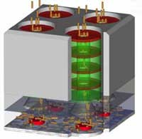 Most of today's rocket engines rely on chemical propulsion. All current spacecraft use some form of chemical rocket for launch and most use them for attitude control as well (the control of the angular position and rotation of the spacecraft, either relative to the object that it is orbiting, or relative to the celestial sphere). Real rocket scientists though are actively researching new forms of space propulsion systems. One heavily researched area is electric propulsion (EP) that includes field emission electric propulsion (FEEP), colloid thrusters and other versions of field emission thrusters (FETs). EP systems significantly reduce the required propellant mass compared to conventional chemical rockets, allowing to increase the payload capacity or decrease the launch mass. EP has been successfully demonstrated as primary propulsion systems for NASA's Deep Space 1, Japan's HAYABUSA, and ESA's SMART11 missions. A new EP concept proposes to utilize electrostatically charged and accelerated nanoparticles as propellant. Millions of micron-sized nanoparticle thrusters would fit on one square centimeter, allowing the fabrication of highly scaleable thruster arrays.
Mar 26th, 2007
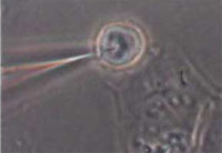 Biosensors, which incorporate biological probes coupled to a transducer, have been developed during the last two decades for environmental, industrial, and biomedical diagnostics. The application of nanotechnology to biosensor design and fabrication promises to revolutionize diagnostics and therapy at the molecular and cellular level. The convergence of nanotechnology, biology, and photonics opens the possibility of detecting and manipulating atoms and molecules using a new class of fiberoptic biosensing and imaging nanodevices. These nanoprobes and nanosensors have the potential for a wide variety of medical uses at the cellular level. The potential for monitoring in vivo biological processes within single living cells, e.g. the capacity to sense individual chemical species in specific locations within a cell, will greatly improve our understanding of cellular function, thereby revolutionizing cell biology. Existing nanoprobes have already demonstrated the capability of performing biologically relevant measurements inside single living cells.
Mar 23rd, 2007
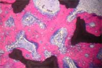 The market for medical implant devices in the U.S. alone is estimated to be $23 billion per year and it is expected to grow by about 10% annually for the next few years. Implantable cardioverter defibrillators, cardiac resynchronization therapy devices, pacemakers, tissue and spinal orthopedic implants, hip replacements, phakic intraocular lenses and cosmetic implants will be among the top sellers. Current medical implants, such as orthopaedic implants and heart valves, are made of titanium and stainless steel alloys, primarily because they are biocompatible. Unfortunately, in many cases these metal alloys with a life time of 10-15 years may wear out within the lifetime of the patient. They also might not achieve the same fit and stability as the original tissue, and in a worst case, the host organism might reject the implant altogether. While available implants can alleviate excruciating pain and allow patients to live more active lives, there often are problems getting bone to attach to the metal devices. Small gaps between natural bone and the implant can increase over time, requiring the need for additional surgery to replace the implant. In the quest to make bone, joint and tooth implants almost as good as nature's own version, scientists are turning to nanotechnology. Researchers have found that the response of host organisms (including at the protein and cellular level) to nanomaterials is different than that observed to conventional materials. While this new field of nanomedical implants is in its very early stage, it holds the promise of novel and improved implant materials.
Mar 22nd, 2007
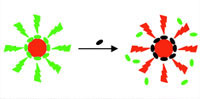 Nanocrystals, also called quantum dots (QD), are artificial nanostructures that can possess many varied properties, depending on their material and shape. For instance, due to their particular electronic properties they can be used as active materials in single-electron transistors. Because certain biological molecules are capable of molecular recognition and self-assembly, nanocrystals could also become an important building block for self-assembled functional nanodevices. The atom-like energy states of QDs furthermore contribute to special optical properties, such as a particle-size dependent wavelength of fluorescence; an effect which is used in fabricating optical probes for biological and medical imaging. So far, the use in bioanalytics and biolabeling has found the widest range of applications for colloidal QDs. Though the first generation of quantum dots already pointed out their potential, it took a lot of effort to improve basic properties, in particular colloidal stability in salt-containing solution. Initially, quantum dots have been used in very artificial environments, and these particles would have simply precipitated in 'real' samples, such as blood. These problems have been solved and QDs are ready for their first real applications.
Mar 21st, 2007
 A few years ago it was discovered that the process of thermal inkjet printing can be applied to fabricate hard tissue scaffolds (such as bones) and, just recently, soft tissue with liquid biomaterials. Research is also underway to use inkjet printing for the fabrication of organic semiconductors, which, because of their low stability, will be targeted at one-time-only applications such as water purity testers. Compared to the research done with respect to organic materials, inkjet printing of inorganic materials for the formation of active devices is relatively rare. To date, only a handful of inorganic materials have been inkjet printed, primarily because of the difficulty in preparing inkjet-printable precursors. Current methods for the production of functional inorganic electronic devices are quite expensive because they require the sequential deposition, patterning, and etching of selected semiconducting, conducting, and insulating materials, involving multiple photolithography and vacuum-deposition processes. Now though, researchers have come up with a process for printable inorganic semiconductors, opening a route to the fabrication of high-performance and ultra low-cost electronics such as transparent electronics and thin film solar cells.
Mar 20th, 2007
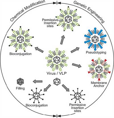 Geneticists regularly use viruses as vectors to introduce genes into cells that they are studying. Viruses are also the most common carrier vehicles in gene therapy. Having been genetically altered to carry normal human DNA, they deliver the therapeutic genes to the patient's target cells. These viruses infect cells, deposit their DNA payloads, and take over the cells' machinery to produce the desirable proteins. Current trends in nanotechnology promise to take virus technology into an entirely new direction. From the viewpoint of a materials scientist, viruses can be regarded as organic nanoparticles. Their surface carries specific tools designed to cross the barriers of their host cells. The size and shape of viruses, and the number and nature of the functional groups on their surface, is precisely defined. As such, viruses are commonly used in materials science as scaffolds for covalently linked surface modifications. The powerful techniques developed by life sciences are becoming the basis of engineering approaches towards nanomaterials, opening a wide range of applications far beyond biology and medicine.
Mar 19th, 2007
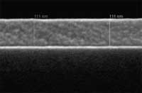
 The assembly of nanoparticles along the external or internal surface of carbon nanotubes (CNTs) is of both fundamental and technological interest. Combining unique properties of CNTs and nanoparticles, the nanoparticle/nanotube composite structure attracts a broad range of advanced applications, including nanoelectronics, chemical and biosensors, catalysis and fuel cells. This so-called 'decoration' of CNTs has been used to increase the hydrogen storage capacity, to make nanotubes magnetic, or to grow secondary structures inside the nanotubes to increase the available surface for catalysis. In the case of interior wall decoration of CNTs, the internal cavity of the nanotube often is obstructed and no flow can be achieved or there could be release of the particles in the environment. In the case of exterior wall decorations, the particles enter in direct contact with the environment and may be lost during the nanotube handling. A novel technique of multifunctional nanotubes with controllable amounts of nanoparticles embedded in their walls during the synthesis process solves both problems leaving the CNT bore accessible and keeping the nanoparticles shielded from the environment by the CNT walls. This paves the way to using carbon nanotubes as nanoscale biological probes for sub-cellular investigation.
Mar 16th, 2007
 Carbon nanotubes (CNTs) have captured the imagination of many scientists and engineers as a result of properties of individual tubes (e.g. very high electrical and thermal conductivities, high stiffness). Things often get 'messy' however, when one tries to make them work collectively, e.g. in composites. Three-dimensional networks of carbon nanotubes are usually made within a supporting material, such as in polymer composite or liquid dispersion. While networks of CNTs have been observed transiently in furnaces with lots of raw nanotube material, such an approach does not permit much experimental control over the resulting network. A novel approach to fabricating CNT networks are CNT aerogels. Aerogels are novel materials in their own right - a material derived from gel in which the liquid component of the gel has been replaced with gas. The result is an extremely low density solid. Microscopically, aerogels are composed of tenuous networks of clustered nanoparticles. These materials often have unique properties due to their very high strength-to-weight and surface-area-to-volume ratios. To date, most aerogels are fabricated from silica or pyrolized organic polymers. Fabricating aerogels with CNTs offers potential for improvement over current carbon aerogel technologies in device applications such as sensors, actuators, electrodes, and thermoelectrics.
Mar 15th, 2007
 Subscribe to our Nanotechnology Spotlight feed