Showing Spotlights 305 - 312 of 624 in category All (newest first):
 Buildings and other man-made structures consume as much as 30-40% of the primary energy in the world, mainly for heating, cooling, ventilation, and lighting. 'Smart' windows are expected to play a significant role in reducing the energy consumption of homes in two ways: by generating energy themselves; and by providing better insulation by allowing light in and keeping the heat out (in hot summers) or in (in cold winters). Vanadium dioxide (VO2) has long been recognized as a a material of significant technological interest for optics and electronics and a promising candidate for making 'smart' windows: it can transition from a transparent semiconductive state at low temperatures, allowing infrared radiation through, to an opaque metallic state at high temperatures, while still allowing visible light to get through. In new work, researchers have now offered a simple method for promoting the production of monoclinic VO2 nanoparticles by doping.
Aug 27th, 2012
 Micro- and nanoporous materials can widely be found in nature, be it zeolite minerals, cell membranes, or diatom skeletons. Researchers are developing artificial analogues of such materials, i.e. nanoporous materials, for industrial applications in areas such as catalysis, water purification, environmental clean-up, molecular separation and proton exchange membranes for fuel cells. Manufacturing nanosieves with straight nanopores is still challenging, especially when the pore size is less than 10 nm. Researchers in Korea have now developed a novel material and fabrication technique that allows easy fabrication of nanosieves with sub-10 nm nanopores with straight pore-structure. With it, controlling the pore size from sub-nm to 5 nm becomes very easy.
Aug 24th, 2012
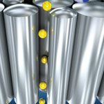
 Nanoporous alumina membranes are used in a wide range of applications, from photonics and sensors to bioelectronics or filtration membranes, since they are basically a 'universal' mold for making zero- or one-dimensional nanostructures of mostly any material or compound. With current fabrication processes, the main limitations of porous alumina templates are their pore size, which cannot be smaller than 25nm, and their polydomain structure, which prevents the possibility of addressing each nanopore individually for electronics applications. A new nanofabrication process by researchers from France and Germany allows to reduce the pore diameter while maintaining the self-ordering and keeping the lattice constant. This led to a new family of AAO templates with identical pores with a diameter below 10nm and a porosity of 3.5%.
Aug 6th, 2012
 Over the past few years, touchscreens have become ubiquitous in the world of mobile electronic devices. A next generation of touch sensing devices will be vastly more advanced and lead to ultrasensitive artificial skins. Another, novel model for advanced man-machine interactive systems could be based on moisture detectors. Here, actual touch is no longer necessary for a positioning interface to react; rather, the distribution of water molecules that exists around all humid surfaces, such as a human finger, would be sufficient to trigger a response. Researchers in China have now demonstrate such a flexible touchless positioning interface based on the spatial mapping of moisture distribution.
Jul 3rd, 2012
 Many nanotechnology projects require some form of nanopatterning technique for fabricating the devices, structures and surfaces required in fields ranging from electronics to photonics, security, biotechnology and medicine. Although they may not be visible to the naked eye, the nanometer-sized trenches, ridges, curves and grooves of these patterns and surfaces have a very visible impact. Researchers have developed a wide range of nanopatterning techniques, from top-down methods such as nanoimprint, e-beam or UV lithography to bottom-up techniques such as transfer nanolithography or nanopositioning on DNA or protein scaffolds. A novel technique uses a biofunctionalization approach based on resist-less electron-beam-induced deposition of carbon-containing nanofeatures, that has been developed into a universal biofunctionalization platform. This unique ability can be exploited for biological experiments, where cells respond to the nanoscale density of activating molecules such as antibodies.
Jun 26th, 2012
 Quantum rings show unique electronic, magnetic and optical properties. These unique properties make them attractive for various applications such as magnetic memory and systems for future quantum computers. To be used in practical applications, however,the quantum rings need to be fabricated in a controlled fashion. So far, the fabrication of laterally ordered quantum rings has not been reported. Now, though, researchers have demonstrated a fabrication method to obtain large scale ordered quantum rings. The quantum rings can be simply created by partially capping quantum dots. The key to fabricating ordered quantum rings is to create ordered quantum dots.
Jun 21st, 2012
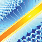
 Physicists have uncovered a new method to manipulate light by borrowing an idea from the field of mathematical topology - topology is the mathematical field dealing with the properties of objects undergoing deformations, such as stretching and twisting. They created an artificial material, a "metamaterial", that can transform from regular dielectric - a substance like glass or plastic, which does not conduct electricity - to a medium that behaves like metal (reflects) in one direction and like dielectric (transmits) in the other. The research team expects optical topological transition to be the basis for a number of applications of both fundamental and technological importance through use of metamaterial-based control of light-matter interaction.
May 9th, 2012
 Thin films comprising carbon-based molecules and polymers have promising technological applications, such as biosensors, solar cells, electrically-active and light-emitting layers for displays, etc. Oftentimes, properties, such as luminescence and conductivity, depend on the orientation of crystals within the film. In organic thin films deposited on substrates, crystallization most often occurs isotropically in the plane of the film. Much research has thus focused on controlling the orientation of crystals in the plane of organic thin films. The use of temperature gradients and gravitational flow have been successfully employed to orient crystals unidirectionally. Two-dimensional control of the orientation of crystals spatially within organic thin films, however, remains exceedingly difficult to achieve. In new work, researchers have now demonstrated a method to guide crystallization along arbitrary patterns in the plane of organic thin films, using an organic semiconductor.
May 8th, 2012
 Subscribe to our Nanotechnology Spotlight feed