Showing Spotlights 449 - 456 of 2783 in category All (newest first):
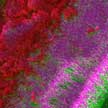
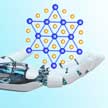 Charge density wave (CDW) is a quantum mechanical phenomenon, which induces distortion in the crystal structures of some low-dimensional (1D or 2D) metals, when the temperature is reduced. Such distorted crystal structure is known as CDW phase and its resistivity is much higher than the original symmetric phase. Since the switching between symmetric and CDW phase can also be made by the application of external electric field, these materials are technologically important and have attracted immense attention in the nanoelectronics community.
Aug 6th, 2020
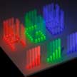 Researchers have fabricated nanoscale color pixels that utilize three-dimensional space to improve and control the brightness of individual pixels with nanoscale lateral dimensions. Specifically, this novel method utilizes 3D printing of vertically freestanding nanostructures containing red, green, or blue light-emitting quantum dots embedded in polymer nanowires. The emission brightness of the pixels linearly increases with the height of the pixels due to the increase in the number of quantum dots due to the increased volume. The 3D geometry enables a 2-fold increase in brightness without causing significant changes in the lateral dimensions of the pixel.
Aug 5th, 2020
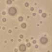 Conventional optothermal microbubble assisted bio-sensing is not suitable for protein sensing due to the high temperatures over 100 dgrees C. To overcome this problem, researchers have demonstrated a proof-of-concept study that reduces the working temperature of bubble generation simply by introducing a volatile, water-immiscible liquid into an aqueous medium. This enables the generation of bubbles at a much lower temperature of around 30 degrees C, not only making this sensing platform compatible with proteins but also enhancing the surface capture of proteins.
Jul 27th, 2020
 Researchers have turned to M13 bacteriophages as a sensing layer for colorimetric sensors. M13 is a nanoscale, benign virus with a shape that closely resembles collagen fibers. It can change its structure by shrinking or expanding in response to a changing surrounding environment. By using a highly lossy resonant promoter as the substrate, the spin-coated M-13 virus layer exhibits strong resonance even with ultrathin thickness variations, resulting in colorimetric behavior with enhanced chromaticity.
Jul 24th, 2020
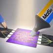 Researchers have fabricated photodetectors on paper by mimicking the action of drawing/writing with a pencil on standard paper. The results indicate that this process can be employed with other layered materials like the semiconducting molybdenum disulfide to fabricate electronic devices on paper. There are many layered materials (so called van der Waals materials) that have similar mechanical properties to graphite and thus are susceptible of being cleaved upon mechanical rubbing against paper substrates.
Jul 23rd, 2020
 Researchers have discovered a novel 'sandwiched' silicon electrode structure that can withstand 500 cycles and deliver capacities three times larger than graphite. They used freestanding sheets made of carbon nanotubes - bucky papers - for sandwiching silicon nanoparticles. These nanotubes form a quasi-three-dimensional structure and hold silicon nanoparticles together even after 100 cycles and mitigate electrical resistance arising from breaking of particles. The sandwiched silicon anode was able to withstand discharging rates as high as 4C.
Jul 22nd, 2020
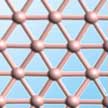 Borophene is the name for atomically thin, two-dimensional (2D) sheets of boron. Whereas boron is a nonmetallic semiconductor in its bulk form, it becomes a metallic conductor in 2D, even at a thickness of only one atomic layer. Among 2D materials, borophene has attracted considerable attention owing to its unique chemical structure and impressive electronic conductivity and surface properties. A recent review of the state of borophene research discusses various growth techniques and application areas for borophene and provides an in-depth summary of the material's electronic, optical, thermal, and elastic properties compared to its 2D cousins.
Jul 21st, 2020
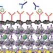 Researchers have designed and fabricated an ultrasensitive plasmonic biosensor with the integration of atomically thin perovskite nanomaterials on metasurfaces. For that purpose, they used an atomically thin perovskite nanomaterial with high absorption rate, sandwiched between hexagonal boron nitride and graphene layers, which enables the precise tuning of the depth of the plasmonic resonance dip. This biosensor can reach an ultra-high plasmonic sensitivity for detecting small-molecule, low-concentration analytes.
Jul 10th, 2020
 Subscribe to our Nanotechnology Spotlight feed