Showing Spotlights 449 - 456 of 624 in category All (newest first):
 Photonic crystals are similar to semiconductors, only that the electrons are replaced by photons (i.e. light). By creating periodic structures out of materials with contrast in their dielectric constants, it becomes possible to guide the flow of light through the photonic crystals in a way similar to how electrons are directed through doped regions of semiconductors. The photonic band gap (that forbids propagation of a certain frequency range of light) gives rise to distinct optical phenomena and enables one to control light with amazing facility and produce effects that are impossible with conventional optics. A prominent example of a photonic crystal is the naturally occurring gemstone opal. The problem with artificial opals, which limits their applications, is that they lack in pattern variety and their fabrication requires very expensive equipment and sophisticated processes. In contrast, natural photonic crystals have various patterns that are quite promising structural matrices for creating novel optical devices. One example are peacock feathers, whose iridescent colors are derived from the 2D photonic crystals structure inside the cortex.
Aug 15th, 2008
 The key to using self-assembly as a controlled and directed nanofabrication process lies in designing the components that are required to self-assemble into desired patterns and functions. Self-assembly reflects information coded in individual components - characteristics such as shape, surface properties, charge, polarizability, magnetic dipole, mass, etc. These characteristics determine the interactions among the components and the whole essence of self-assembly arises from these dynamic properties. In this respect, many self-assembled nanostructures show to be responsive to external stimuli such as temperature, pH, or solvent polarity. An exciting field for nanotechnology researchers is the challenge of extending the scope of nanostructures with stimulus-responsive properties towards the fabrication of 'smart' nanoscale materials. New work by Korean scientists demonstrates that simple addition of small guest molecules triggers reversible structural transformation. The novelty of this research is that, so far, switching of material properties triggered by external stimuli via nanoscale objects had not been realized yet.
Aug 11th, 2008
 Remember the movie blockbuster Erin Brockovich? The film is based on a real world legal case that revolves around hexavalent chromium, also known as chromium (VI), used by the Pacific Gas and Electric Company to control corrosion in cooling towers in its Hinkley, CA compressor station. Chromium (VI), a natural metal, is known to be toxic and is recognized as a human carcinogen via inhalation. It also is widely used by industry in the manufacture of stainless steel, welding, painting and pigment application, electroplating, and other surface coating processes. Researchers in Germany now have developed a novel method of multilayer anticorrosion protection including the surface pre-treatment by sonication and deposition of polyelectrolytes and inhibitors. This method results in the formation of a smart polymer nanonetwork for environmentally friendly organic inhibitors.
Jul 29th, 2008
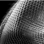 The use of design concepts adapted from nature is a promising new route to the development of advanced materials. There are quite a number of terms such as biomimetics, biognosis, biomimicry, or even 'bionical creativity engineering' that refer to more or less the same thing: the application of methods and systems found in nature to the study and design of engineering systems and modern technology. And increasingly, nanotechnology researchers find naturally occurring nanostructures a useful inspiration for overcoming their design and fabrication challenges. Because biological structures are the result of millennia of evolution, their designs possess many unique merits that would be difficult to achieve by a completely artificial simulation. By replicating the eye of a fruit fly, researchers have now demonstrated a highly reliable and low-cost technique for making inorganic replicas of biotemplates for fabricating complex nanostructures with biologically inspired functionality.
Jul 24th, 2008
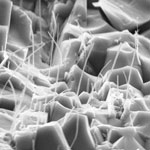 Having come a long way from pottery and tableware, modern advanced ceramics are high-performance materials that find use in things such as bio-medical implants, jet engine turbine blades, superconductors, missile nose cones, scratch-proof watches, or the heat protection tiles used on the Space Shuttle. Super-tough and ultra-high temperature resistant materials are in critical need for applications under extreme conditions such as jet engines, power turbines, catalytic heat exchangers, military armors, aircrafts, and spacecrafts. Structural ceramics have largely failed to fulfill their promise of revolutionizing engines with strong materials that withstand very high temperature. The major problem with the use of ceramics as structural materials is their brittleness. Although many attempts have been made to increase their toughness, including incorporation of fibers and particles, currently available ceramics and their composites are still not as tough as metals and polymers. The brittleness of ceramic materials has not yet been overcome and it has proven difficult to solve this problem by conventional material engineering approaches. The extraordinary mechanical properties of carbon nanotubes (CNTs) have generated strong research interest in their possible use in reinforced composite materials because incorporating CNTs into a ceramic matrix might be expected to produce tough as well as highly stiff and thermostable ceramic composites.
Jul 17th, 2008
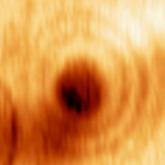 Electrometers are instruments that measure electric charge or electrical potential difference by means of electrostatic force. While early electrometers such as developed by Lord Kelvin in the 19th century were crude instruments, modern electrometers based on solid state technology are high-precision electronic devices that, in extreme cases, are so sensitive they can count individual electrons as they pass through a circuit. As the dimensions of electronic devices shrink further, the probes required to measure the voltage inside a miniature conductor have to be miniaturized, too. An alligator clip cannot be scaled down indefinitely to perform such tasks. Furthermore, as devices reach the nanoscale, the perturbation of the measurement on the device itself cannot be neglected and must be assessed. A few techniques, many of which are based on scanning a small object such as an atomic force microscope (AFM) tip, have been developed in the past to address this challenge. Each technique has its pros and cons.
Jul 14th, 2008
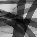
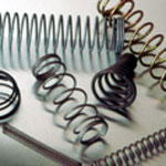 Elastomeric (i.e. elastic) proteins are able to withstand significant deformations without rupture before returning to their original state when the stress is removed. Consequently, these proteins confer excellent mechanical properties to many biological tissues and biomaterials. Depending on the role performed by the tissue or biomaterial, elastomeric proteins can behave either as springs or shock absorbers. Recent scientific work in Canada resulted in the engineering of the first artificial chameleon elastomeric proteins that mimic and combine these two different behaviors into one protein. Under the regulation of a molecular regulator, these designer proteins exhibit one of the two distinct mechanical behaviors - spring or shock absorber - which closely mimic the two extreme behaviors observed in naturally occurring elastomeric proteins.
Jul 2nd, 2008
 The reduction of linewidth is one of the most important problems in integrated circuit (IC) technology because the speed and performance of computer chips is dictated by the lithographic minimum printable size. In the early 1960s, ICs had a linewidth of about 5 micrometers. Dramatic improvements in optical lithography technology has brought this down to the limits allowed by the wavelength of light that is used in the process. Current state-of-the-art photolithography tools use deep ultraviolet light with wavelengths of 248 and 193 nm, which theoretically allow minimum feature sizes down to 50 nm. But even the shortest UV wavelength currently in use (157 nm) does not provide the resolution required by the ever decreasing feature sizes of state-of-the-art nanomanufacturing processes. Researchers in Israel have been working on the use of laser ablation to write very small features - much smaller than the optical wavelength - on the surface of different materials. They have now demonstrated floating tip nanolithography, a high quality non-contact surface modification with high spatial resolution within a commercial atomic force microscope.
Jul 1st, 2008
 Subscribe to our Nanotechnology Spotlight feed