| Posted: Jun 16, 2015 |
Stacking semiconductors for artificial photosynthesis
|
|
(Nanowerk News) A new material with light absorption characteristics ideally suited for making chemical fuels from sunlight was created via a nanowire growth strategy that fused the semiconductors silicon (Si) and gallium arsenide (GaAs) together in a new way. The GaAs nanowire array increases optical absorption by trapping the incident light and has potential for high solar energy conversion efficiency (Energy and Environmental Science, "Optical, electrical, and solar energy-conversion properties of gallium arsenide nanowire-array photoanodes").
|
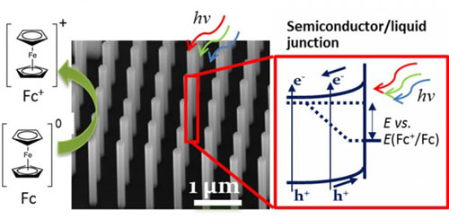 |
| Gallium arsenide nanowire arrays grown on a silicon substrate are studied using photoelectrochemistry. The middle photograph shows a scanning electron micrograph of a vertically aligned nanowire array; the figure on right is the band energy diagram of the rectifying nanowire/liquid junction; the figure on the left illustrates oxidative redox reactions of ferrocene to ferrocenium molecules at nanowire surfaces.
|
|
The Impact
|
|
This research demonstrates that it is possible to join Si and GaAs, two semiconductors that optimally absorb a different portion of the solar spectrum, to create two high energy species that can catalyze different chemical reactions. Such an arrangement may enable the development of a device that generates storable solar fuels by splitting water into hydrogen and oxygen using fused semiconductors.
|
|
Summary
|
|
The intermittent nature of sunlight makes it desirable to store solar energy in the form of chemical fuels, as nature accomplishes through photosynthesis. The light-driven electrolysis or “splitting” of water can be used to produce hydrogen gas, a transportable fuel that can be utilized without carbon emissions.
|
|
However, it has been difficult to develop materials that absorb a large portion of the solar spectrum yet still have sufficient energy to drive water electrolysis.
|
|
To address this challenge, researchers at the Joint Center for Artificial Photosynthesis, an Energy Innovation Hub, and the Center for Energy Nanoscience, an Energy Frontier Research Center, combined efforts to grow GaAs nanowires on Si substrates. The Si-GaAs nanowire design enables two semiconductors to optimally absorb different portions of the solar spectrum, creating two species that could potentially produce oxygen with one semiconductor and hydrogen with the other.
|
|
The sequential stacking of the highly efficient GaAs and Si semiconductors produced the light absorption, photovoltage, and high current densities needed for the water-splitting reaction in an artificial photosynthesis system.
|
|
This experimental approach could be used to develop new devices incorporating multiple semiconductors to achieve light-driven water electrolysis.
|