| Posted: | |
| (Nanowerk Spotlight) Ferroelectric domain patterns attract increasing attention owing to their potential for integrated optical and novel electronic applications. Lately, Piezoresponse Force Microscopy (PFM) has become a standard technique for the investigation of such domain patterns due to the high lateral resolution of only about 10 nm even – so no specific sample preparation is needed (see for instance: "Putting the squeeze on a crystal leads to novel electronics "). In addition, due to the frequency modulated PFM technique for recording ferroelectric domains, topography and domain patterns can be recorded simultaneously and independently. | |
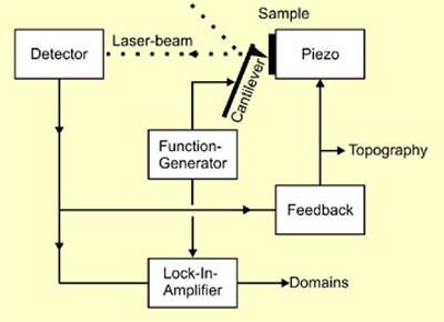
| Piezoresponse force microscopy is based on the deformation of the sample due to the converse piezoelectric effect. Therefore a scanning force microscope is operated in contact mode with an alternating voltage applied to the tip. In piezoelectric samples this voltage causes thickness changes of the sample and therefore vibrations of the sample surface which lead to oscillations of the cantilever that can be read out with a lock-in amplifier. | |
 |
|
| Electronic circuit for PFM operation. (Image: Dr. Elisabeth Soergel, University of Bonn) | |
| "Although straight forward at first sight, PFM measurements gave rise to a wealth of discussions mainly due to their strong frequency dependence which lead to alternative explanations of the origin of the domain contrast," Dr. Elisabeth Soergel explains. "Above all, another name was introduced for one and the same method (dynamic contact electrostatic force microscopy)." | |
| Soergel is a researcher and lecturer at the University of Bonn's Institute of Physics where one of her research foci is the visualization of ferroelectric domains with PFM. | |
 |
|
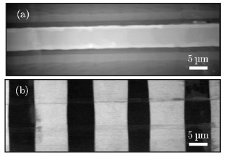
| Topography (a) and simultaneously recoded piezoresponse (b) of a titanium implanted waveguide in a periodically poled lithium niobate (PPLN) crystal. Image recording was performed with the SMENA SPM by NT-MDT and probes of type DCP11 were used. (Sample courtesy: University of Paderborn) | |
| Generally, all scanning force microscopes are suited for PFM operation as long as they allow application of voltages to the tip and separate readout of the cantilever movement. The scanning velocity has to be adapted to the rise time of the lock-in amplifier. | |
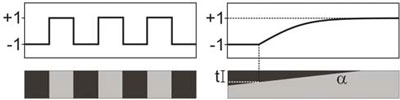
| An attractive aspect of PFM is that it allows not only for detailed information of the areal configuration but also of the depth of the domains. Therefore a bulk domain structure, e. g. periodically poled lithium niobate (PPLN) in a 500 µm thick crystal, is used as a reference sample (PPLN is a domain-engineered lithium niobate crystal, used mainly for achieving quasi-phase-matching in nonlinear optics). | |
 |
|
| PPLN (left) and domain wedge (right) for calibration of the depth resolution in PFM. The visible depth t is 1.7 µm for probes with 70 nm tip radius. (Image: NT-MDT) | |
| From comparative measurements of the domain contrast using the PPLN and the shallow domains to be investigated one can ascertain their depth. This measurement is very sensitive to the tip radius of the probe used and therefore diamond coated tips that show a very long living without abrasion are preferable. For instance, using DCP11 probes from NT-MDT with a nominal radius of ∼70 nm allows for a depth profiling of shallow domains up to t = 1.7 µm (figure above). | |
| Interestingly, this value is independent of the material investigated, i. e. the visible depth is the same for every material. In order to allow for depth evaluation over a larger range, probes with larger tip radius are required, thereby renouncing the high lateral resolution which can only be obtained with sharp tips. | |
| Besides its application for integrated circuit applications where surface domain patterns are highly desired, knowledge of the depth resolution with PFM is also essential when investigating piezoresistive ceramics where the typical size of the single particles is of the order of only 100 nm, thus much less then the visible depth. Consequently, PFM imaging ceramics generally not only displays the top layer but contributions of underlying particles alter the obtained contrast. | |
 By
Michael
Berger
– Michael is author of three books by the Royal Society of Chemistry:
Nano-Society: Pushing the Boundaries of Technology,
Nanotechnology: The Future is Tiny, and
Nanoengineering: The Skills and Tools Making Technology Invisible
Copyright ©
Nanowerk LLC
By
Michael
Berger
– Michael is author of three books by the Royal Society of Chemistry:
Nano-Society: Pushing the Boundaries of Technology,
Nanotechnology: The Future is Tiny, and
Nanoengineering: The Skills and Tools Making Technology Invisible
Copyright ©
Nanowerk LLC
|
|
|
Become a Spotlight guest author! Join our large and growing group of guest contributors. Have you just published a scientific paper or have other exciting developments to share with the nanotechnology community? Here is how to publish on nanowerk.com. |
|