| Aug 05, 2020 | |
3D-printed nanoscale color pixels improve brightness control |
|
| (Nanowerk Spotlight) A pixel – which actually is short for 'picture element' – is the smallest unit used to record or display a digital image. For instance, if your camera has an 8 megapixel sensor, that means it has a resolution of 3,264 x 2,448 pixels, i.e. there are close to 8 million pixels on that sensor chip. | |
| The more pixels on a given area the higher the density of the integrated information, such as the resolution of displays. If the size of an area is limited, the only way to increase resolution (i.e. the number of pixels) is by reducing pixel size. | |
| Most methods used for producing display pixels are based on the two-dimensional (2D) patterning of light-emitting materials, such as inkjet printing, electrohydrodynamic jet (e-jet) printing, intaglio transfer printing, and photolithography. | |
| "These 2D methods often suffer from reduced brightness at higher pixel densities owing to the decreased volume and its interactions with the excitation source," Dr. Jaeyeon Pyo, a Senior Researcher at Korea Electrotechnology Research Institute (KERI), tells Nanowerk. "Although repeated printing processes can improve brightness by increasing the thickness of the 2D pixels, the concomitant broadening in the lateral directions limits the obtainable thickness as well as the pixel density." | |
| Pyo and his collaborators from KERI now have fabricated nanoscale color pixels that utilize three-dimensional (3D) space to improve and control the brightness of individual pixels with nanoscale lateral dimensions. Specifically, this novel method utilizes 3D printing of vertically freestanding nanostructures containing red, green, or blue light-emitting quantum dots (with a size of 620 nm) embedded in polymer nanowires. | |
| The team reported their findings in ACS Nano ("3D-Printed Quantum Dot Nanopixels"). | |
| "We figured out that the emission brightness of the pixels linearly increases with the height of the pixels due to the increase in the number of quantum dots due to the increased volume," Pyo explains. "The 3D geometry enables a 2-fold increase in brightness without causing significant changes in the lateral dimensions of the pixel. We can control the brightness by adjusting the pixel height in accordance with the observed linear relation between brightness and height." | |
 |
|
| Three-dimensional printing of nanopixels. (a) Conceptual drawing of 3D-printed nanopixels. (b) Schematic and bright-field optical images representing the procedure of 3D nanopixel printing. Scale bar: 5 µm. (Reprinted with permission by American Chemical Society) (click on image to enlarge) | |
| As shown in the figure above, the team fabricated 3D-shaped nanoscale color pixels by printing R, G, or B color-emitting nanophotonic inks (with peak emission wavelengths at 650, 540,and 480 nm, respectively) in the direction perpendicular to a substrate. | |
| The 3D-printed nanopixels are essentially sub-micrometer dot pixels when viewed from the top or bottom of the substrate. However, the pixels' 3D shape enables enhanced interaction with the excitation source while maintaining the same width, which means without degrading the pixel density. | |
| To achieve nanoscale 3D printing, the researchers employed a precise and versatile meniscus-guided 3D nanoprinting method using a glass nanopipette as a nozzle – a technique they reported previously (Advanced Optical Materials, "3D Printed Nanophotonic Waveguides"). | |
| In this present work, they further developed the meniscus writing method for printing photoluminescent nanowires in 3D layouts to produce nanoscale color pixels. | |
 |
|
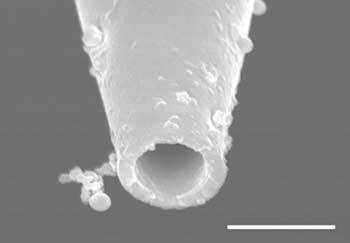
| Scanning electron microscope (SEM) image of a representative nano pipette nozzle. Scale bar: 1 µm. (Reprinted with permission by American Chemical Society) | |
| "We also visualized and studied the narrow directional emissions from the nanoscale pixels regardless of the pixel height," Pyo notes. "For 3D printing, we found that rheological properties of the inks can strongly affect the final morphologies of the printed objects. We also found that increasing the contents of quantum dots in the inks can increase the brightness of the printed pixels, but the uniformity can be reduced at high concentration of quantum dots due to aggregation." | |
| According to the researchers, this technology can provide super high-resolution devices based on the demonstrated nanoscale pixels of about 5600 ppi. | |
| Although the pixel density of recent mobile phones (∼800 ppi) already exceeds the spatial resolution of human eyes, there still are many applications that require much higher densities: Virtual Reality displays require 2000 ppi to be displayed through the magnifying lens, and still further development is required to resolve '3D motion sickness' or 'screen door effect'. Beam projectors can use such high-resolution display panels to project from small panel to the screen as 4K or 8K resolution. 3D nanopixels also can be used in anti-counterfeit or security printing. | |
| Having demonstrated 3D patterning of photoluminescent materials for backlit displays in this work, the team's next target is to develop electrically driven display devices for active-matrix displays. | |
 By
Michael
Berger
– Michael is author of three books by the Royal Society of Chemistry:
Nano-Society: Pushing the Boundaries of Technology,
Nanotechnology: The Future is Tiny, and
Nanoengineering: The Skills and Tools Making Technology Invisible
Copyright ©
Nanowerk LLC
By
Michael
Berger
– Michael is author of three books by the Royal Society of Chemistry:
Nano-Society: Pushing the Boundaries of Technology,
Nanotechnology: The Future is Tiny, and
Nanoengineering: The Skills and Tools Making Technology Invisible
Copyright ©
Nanowerk LLC
|
|
|
Become a Spotlight guest author! Join our large and growing group of guest contributors. Have you just published a scientific paper or have other exciting developments to share with the nanotechnology community? Here is how to publish on nanowerk.com. |
|