-
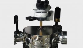
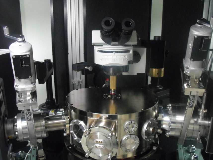
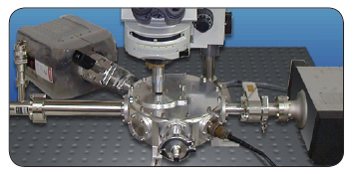
The Cryoview enables measurements of low temperature electrical, optical, magnetic, and thermal properties of materials fully integrated with near-field and far-field optics, Raman, and fluorescence spectroscopies. It opens new avenues for multiprobe measurements including transport properties of materials at temperatures as low as 10K. The CryoView is an award-winning, must-have tool especially suited to probe 2D materials such as graphene, MoS2, BN, TaS2, NBSe2, WS2, HfO2, metamaterials, and metasurfaces as well as other functional material materials such as Si, carbon nanotubes, III-V semiconductors, and quantum dots. -
Nanonics Imaging Ltd. provides near-field optical microscopes (NSOM or SNOM) and atomic force microscopes (AFM). The company offers photonics and plasmonics, defect analysis solutions, dual optical microscopes, scanning stages, and scanned probe microscopy (SPM) probes and nanotools. It also provides NSOM and SPM accessories, such as liquid cells, environmental chamber and nanochemical/gas delivery systems, vibration isolation platforms, APD controllers, double APD detection systems, and NSOM and SPM heads for customized sample stages. The company’s SPM and NSOM systems comprise NSOM (SNOM) systems for transmission, collection, and true reflection NSOM imaging; Raman systems; tip-and sample-scanning probe systems for AFM/Raman/tip enhanced Raman spectroscopy and NSOM/ANSOM applications; photonics/plasmonics workstations that are designed to address nano/micro photonic characterization; fountain pen nanolithography package for chemical writing of liquids and gases; and integrated SPM with electron and ion beam microscopes. Its products are used in chemical sciences, lens characterization, life sciences, microelectronics, nanochemistry, photonics and telecommunication, physics, polymers, Raman, semiconductors, and TFT display applications. Nanonics Imaging Ltd. was founded in 1997 and is headquartered in Jerusalem, Israel.
Visit company website