-
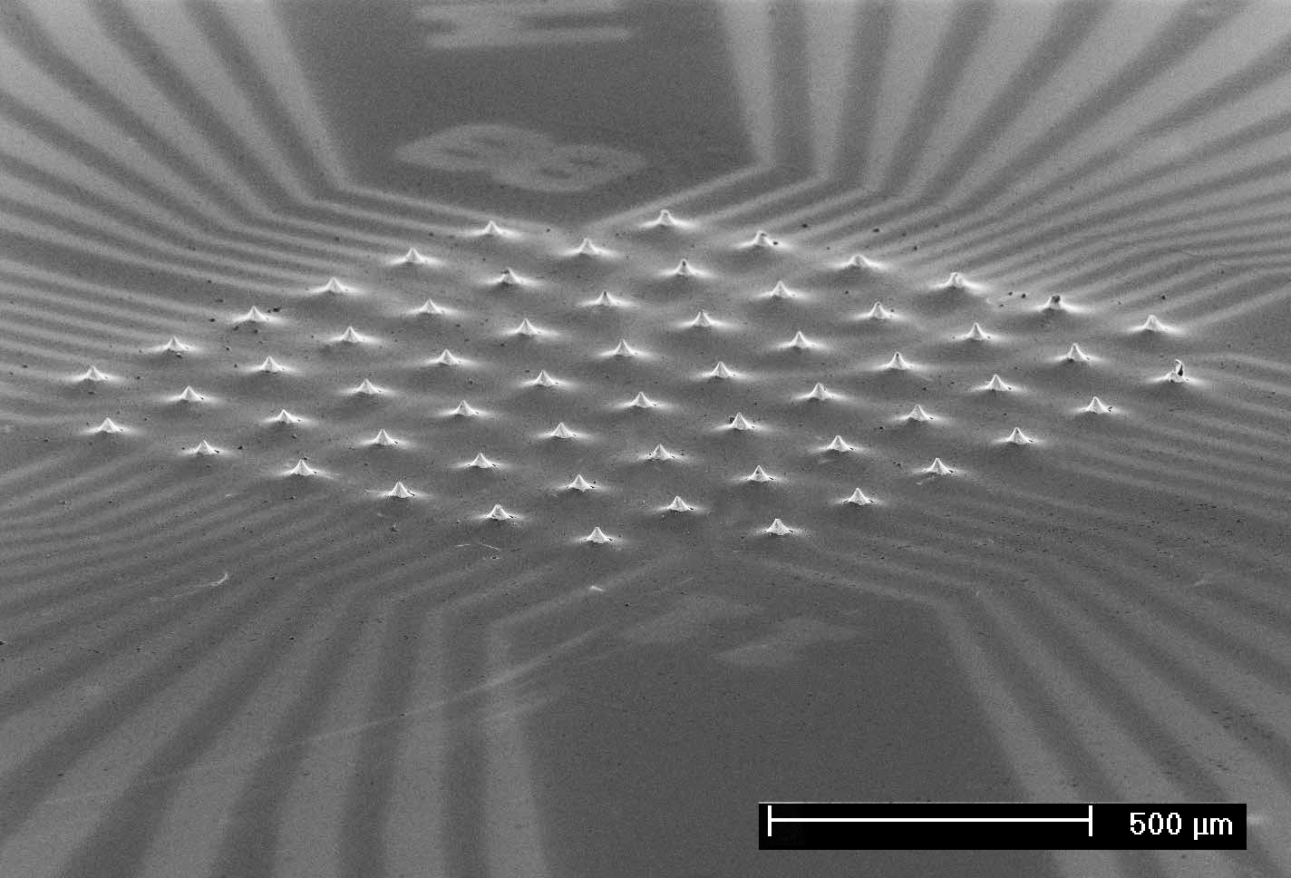
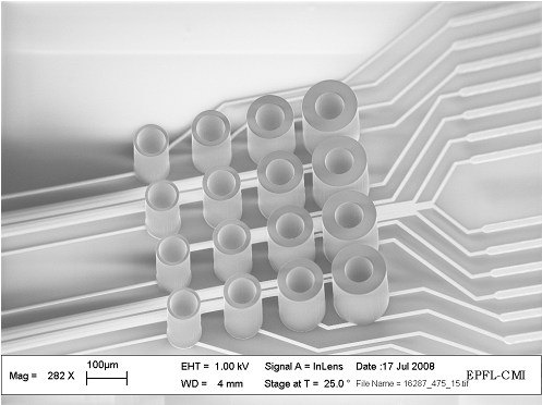
SU8 Photo resist
Performances
• High resolution • Vertical sidewalls • Aspect ratio up to 30 by standard UV lithography • Short bake time
Applications
• Dielectric layer with high resolution and complex shape for transistors passivation/interlayer • Coating by Spray, Inkjet, E-Beam • Display and flexible display • Planarisation layers for AMOLED • MEMS, BioMEMS, NanoMEMS, Microfluidics
Thickness range:
<0.2μm - 400μm
If you wish to speak to our sales or applications team please email [email protected] or visit www.emresist.com -
.png)
EM Resist Ltd. is specialised in developing materials used for lithography and nanofabrication applications. With over 30 years combined experience, we are continually developing the next generation of materials that will enable you to push forward in your research and development.
Can we help you?
Do you have a specific application or problem that you are trying to solve? Are conventional tools or materials not working for you? Let us know and we may be able to help. With our deep in house knowledge on electron beam lithography and close connection with our sister companies EM Analytical & EM Systems Support, we can help you design materials and tools specific for your application.
We have a full suite of nanofabrication tools that are available for one-off project work or complete proof of principle projects.
Visit company website