The Different Types of Lithography in Nanotechnology
Content
The ability to create intricate, nano-scale patterns is at the heart of nanotechnology, and lithography techniques are the tools that make this possible. From photolithography to FIB, each technique offers unique capabilities that can be harnessed for specific applications. As the field of nanotechnology continues to evolve, these techniques will also progress, adapting and improving to meet the increasing demand for smaller, more efficient nanodevices.
Lithography as an Enabler
Nanotechnology is an interdisciplinary science that operates at the nanoscale, typically dealing with structures less than 100 nanometers in size. The ability to manipulate materials at this scale has revolutionized numerous fields, from electronics and medicine to energy and materials science.
A significant enabler of this manipulation is lithography. Derived from the Greek words 'lithos' meaning 'stone' and 'graphein' meaning 'to write', lithography was initially a method of printing images onto paper using stone templates.
Specifically, lithography is a planographic printmaking process in which a design is drawn onto a flat stone (or prepared metal plate, usually zinc or aluminum) and affixed by means of a chemical reaction (watch the process here).
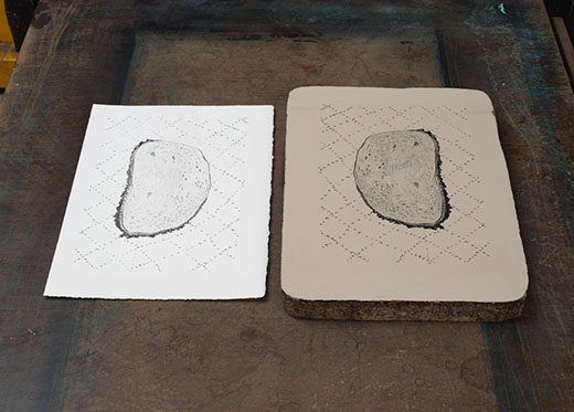
Lithograph on stone (Image: The Met)
The invention of lithography dates back to the end of the 18th century, with the work of Aloys Senefelder, a German author. He discovered that he could write on a smooth limestone with a greasy material and then print images onto paper. The technology further evolved in the 20th century, becoming an integral part of the printing industry. By the mid-20th century, with the rise of the semiconductor industry, lithography found a new application. It became a key process for transferring electrical circuit patterns onto semiconductor wafers, paving the way for the microelectronics revolution.
As our ability to shrink electronic devices improved, so did our need for more refined lithographic techniques. The advent of nanotechnology further propelled this need, leading to the development of various forms of lithography that can pattern features at the nanoscale. From its humble origins in stone printing, lithography now forms the cornerstone of modern technology, underpinning the fabrication of everything from microprocessors and memory chips to digital displays and solar panels. Its ability to pattern at the micro- and nanoscale has played a significant role in enabling Moore's Law, which posits that the number of transistors on a chip doubles approximately every two years.
The different types of lithography, each with their unique capabilities, serve as key tools for scientists and engineers to create and manipulate structures at the nanoscale. This article delves into the various types of lithographic techniques, providing insight into their workings, applications, and future developments.
The Concept and Evolution of Lithography in Nanotechnology
Lithography in the context of nanotechnology is a process that takes its foundational principles from the lithography used in the printing industry but tailors them to the demands of creating structures at the nanoscale. This technique has evolved from simple stone printing to advanced nanofabrication, enabling the design and creation of devices with features much smaller than the width of a human hair.
In its modern form, lithography in nanotechnology involves creating intricate patterns on a substrate, often a thin film of silicon or other semiconducting materials. The substrate is typically coated with a light-sensitive material called a photoresist. By controlling where the photoresist is exposed to light (or other forms of energy such as electrons or ions), specific patterns can be created. These patterns form the basis for various micro- and nanoscale structures, which are used in a broad array of devices.
The evolution of lithography in nanotechnology has been a response to the needs of the semiconductor industry and the field of nanotechnology. As these fields have sought to create smaller, more complex, and more efficient devices, lithography techniques have had to evolve to keep pace. For example, photolithography, which uses light to expose the photoresist, has been the workhorse of the semiconductor industry for many years. However, the size of the features it can create is limited by the wavelength of the light used, leading to the development of techniques such as electron beam lithography and extreme ultraviolet lithography, which can create much smaller features.
The importance of lithography for nanotechnology research and applications cannot be overstated. It is a critical tool for researchers and industries working at the nanoscale, enabling them to translate their designs into tangible devices and structures. As we continue to push the boundaries of what is possible at the nanoscale, it is clear that lithography will remain a key enabler, driving innovation and advancement in the field.
Photolithography, a prevalent method in semiconductor manufacturing, relies on light to transfer geometric patterns from a mask to a light-sensitive chemical, known as a photoresist, on a substrate. It's often referred to as optical lithography due to its reliance on light, and it's a technique that has been integral to the semiconductor industry for decades.
The process begins by coating a substrate, typically silicon, with a layer of photoresist. The photoresist can be of two types: positive or negative. Positive photoresists become soluble when exposed to light and can thus be washed away, leaving the desired pattern behind. On the other hand, negative photoresists react oppositely; the light-exposed regions harden and become insoluble, forming the pattern after the unexposed areas are washed away.
Once the photoresist is applied, a mask with the desired pattern is placed between a light source and the substrate. As the light passes through the mask, it exposes the photoresist to the pattern, which is subsequently developed to reveal the desired structure. The exposed substrate can then be subjected to further processes such as etching or ion implantation to create the final structure.
Photolithography has been fundamental to the evolution and growth of the microelectronics industry, enabling the production of increasingly dense integrated circuits and fulfilling the prediction of Moore's Law. However, photolithography's resolution - the smallest feature size it can create - is ultimately limited by the wavelength of the light used and the numerical aperture of the optical system, a relationship described by the Rayleigh criterion. For many years, the industry has pushed this limit by using shorter wavelengths of light and immersion lithography, where a liquid is used between the lens and the wafer to increase the numerical aperture.
Photolithography: Step by step
Despite these advancements, traditional photolithography techniques struggle to meet the demands of cutting-edge semiconductor processes that require feature sizes smaller than the wavelength of deep ultraviolet light. This has spurred the development of next-generation lithography techniques such as extreme ultraviolet lithography (EUVL), which uses even shorter wavelengths of light to achieve smaller features.
However, photolithography's broad applicability, relatively low cost, and high throughput keep it at the forefront of semiconductor manufacturing, even as newer techniques are being developed.
Electron Beam Lithography (EBL)
Electron Beam Lithography (EBL) is a sophisticated method of lithography that was introduced in the late 1960s as an alternative to photolithography, addressing the need to create smaller structures on substrates. Instead of using light to expose the resist, EBL employs a focused beam of electrons. The significantly smaller wavelength of electrons compared to light allows for higher resolution patterning, enabling the creation of features that can be smaller than 10 nanometers.
The EBL process begins much like other lithography methods, with a substrate coated in a resist. The resist in this case is sensitive to electrons. An electron beam is then focused onto the surface of the resist. The beam is scanned across the resist, and its position is controlled to draw out the desired pattern.
The interaction of the electron beam with the resist changes the resist's solubility. In the case of a positive resist, the exposed regions become more soluble and can be washed away in the developing process, leaving behind the unexposed resist as the final pattern. For negative resists, the situation is reversed: the exposed regions become less soluble, leaving them behind after development.
One of the primary advantages of EBL is its ability to create highly intricate and custom patterns with high resolution, which makes it an invaluable tool in research and development and for creating prototypes. Furthermore, the absence of a physical mask provides more flexibility for design changes, as alterations can be made directly in the electron beam control program, unlike photolithography where a new mask would need to be fabricated.
Probing the resolution limits of electron-beam lithography, researchers have achieved fabrication of 2 nm feature size and 10 nm periodic dense structures, which are the highest resolution patterns ever achieved with common resists. The minimum feature size, 2 nm, is composed of roughly 10 atoms wide, and with just a few atoms of standard deviation.
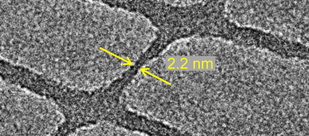
Top-down image obtained using a transmission electron microscope of a 2 nm feature (dark region) fabricated using 200 keV electrons in a scanning transmission electron microscope. (Image: Prof. Karl Berggren, MIT)
However, the benefits of EBL come with trade-offs. The technique is relatively slow since it works by scanning an electron beam across the resist line by line, which makes it less suitable for high-volume manufacturing. Also, the equipment and operating costs for EBL are high due to the need for high-voltage electron sources, ultra-high vacuum conditions, and advanced electron optics.
Despite these limitations, EBL has played a crucial role in nanotechnology, enabling the fabrication of nano-sized devices and structures that would be challenging or impossible to create with other lithography techniques. It has also been instrumental in the development and production of high-end photomasks used in photolithography.
Nanoimprint Lithography (NIL)
Nanoimprint Lithography (NIL) was (proposed by Prof. Stephen Y. Chou of Princeton University in 1995 as a simple, low-cost, and high-throughput method for producing nanoscale patterns. It is a form of contact lithography that directly transfers a pattern from a template or mold onto a substrate coated with a resist, typically a monomer or polymer layer.
Unlike photolithography and electron beam lithography, which utilize light or electron beams to modify the resist's properties, nanoimprint lithography mechanically deforms the resist using a stamp or mold with the desired pattern. The process involves three main steps: resist application, imprinting, and development.
First, the resist is applied onto the substrate. The resist is usually thermoplastic, meaning it softens under heat, or a UV-curable resist. The mold, which is often made of silicon or quartz, is then pressed into the resist, physically deforming it into the desired pattern. If a thermoplastic resist is used, the substrate and resist are heated above the resist's glass transition temperature to make it malleable. In the case of a UV-curable resist, the mold is transparent, and UV light is applied through the mold to cure and harden the resist during the imprinting stage.
Once the resist has been imprinted and cooled (or cured), the mold is removed, leaving the patterned resist behind. Any residual resist layer is then etched away to expose the underlying substrate in the patterned regions, allowing for further processes such as material deposition or etching to create the final nanostructure.
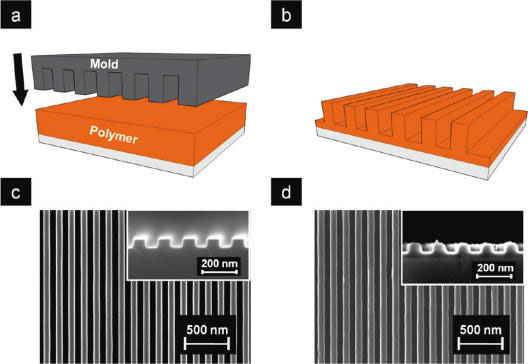
Process flow of thermal nanoimprint lithography: schematic of (a) a mold is pressed onto a thin layer of polymer on a substrate heated to a temperature above the polymer's glass transition temperature, and (b) polymer nanostructures of negative replication to the mold are formed after demolding. SEM images of (c) Si nanolined mold and (d) imprinted P3HT nanogratings. (Reprinted with permission from American Chemical Society)
The primary advantage of NIL is its ability to pattern small feature sizes (down to the sub-10 nm level) with high throughput and at a relatively low cost. Because the pattern is physically transferred from the mold to the resist, NIL is not limited by the diffraction or interference effects that limit the resolution of optical and electron-beam lithography. Moreover, NIL can pattern large areas in a single step, making it a faster process for creating repeating patterns.
However, NIL does have its drawbacks. The requirement for physical contact between the mold and the resist can lead to defects due to particles on the substrate or mold, and the molds themselves can wear down over time. In addition, NIL is a "hard" lithography technique, meaning that once the mold is made, the pattern cannot be changed without creating a new mold. Despite these challenges, NIL has been successfully applied in various fields, including microelectronics, photonics, and data storage, and is being explored for use in emerging areas like bio-nanotechnology.
X-Ray Lithography (XRL)
The limitations of photolithography in terms of resolution, as defined by the Rayleigh criterion, led to the exploration of alternative lithography techniques that use shorter wavelengths of radiation to achieve higher resolution patterning. X-ray lithography, which uses X-rays to expose the resist, was one of these alternatives. The idea of the XRL was first proposed by H. Smith and Spears in 1972 and gained the attention of the micro- and nanofabrication community due to its shorter wavelength and larger penetration depth than conventional UV lithography, offering new possibilities to build micro-devices with high aspect ratio, thick resists, and almost vertical sidewalls.
X-ray lithography follows similar steps to photolithography but replaces the light source with X-rays and uses a special resist that is sensitive to X-rays. Instead of a transparent mask used in photolithography, X-ray lithography uses a mask composed of an X-ray absorbing material patterned on a thin membrane that is X-ray transparent, often made of low atomic number elements like silicon or boron.
The process begins by placing the X-ray mask in close proximity to the resist-coated substrate. When X-rays are directed onto the mask, they are absorbed by the mask’s patterned areas and transmit through the unpatterned areas. The transmitted X-rays expose the resist underneath, and the exposed areas can then be developed to reveal the desired pattern.
Due to the shorter wavelength of X-rays compared to visible light, X-ray lithography can achieve higher resolution patterns than traditional photolithography. It also has excellent depth of focus, which makes it an excellent choice for patterning high-aspect-ratio structures, such as the tall, narrow features found in micro-electro-mechanical systems (MEMS).
However, X-ray lithography requires a synchrotron source to generate the X-rays, which is large, expensive, and complex to operate. The process must also be performed under vacuum conditions to prevent X-ray scattering by air molecules, adding to the complexity and cost of this technique. Despite these challenges, X-ray lithography has found applications in specialized areas like MEMS, power devices, and advanced packaging, where the benefits of high resolution and depth of focus outweigh the additional costs and complexities.
Extreme Ultraviolet Lithography (EUVL)
Extreme Ultraviolet Lithography (EUVL) is the latest advancement in lithographic techniques used in the semiconductor industry. It was developed as a solution to the ongoing demand for higher resolution in microelectronics manufacturing, as existing techniques, such as photolithography, started reaching their physical limits. EUV lithography was first included in the next-generation lithography road maps in the early 90s, but the path to commercialization has been challenging due to the complexities and costs associated with the technology.
The key feature of EUVL is the use of extreme ultraviolet (EUV) light, with a wavelength of 13.5 nm - much shorter than the deep ultraviolet light used in traditional photolithography. This shorter wavelength allows for the patterning of much smaller features, reaching into the single-digit nanometer scale, and it is anticipated to be crucial for semiconductor manufacturing nodes of 5 nm and below.
In EUVL, a laser is directed at a small droplet of tin, which creates a plasma that emits EUV light. This light is collected, focused, and reflected off a series of mirrors before passing through the reticle (analogous to a mask in photolithography), which holds the pattern to be transferred onto the wafer. The EUV light is then reflected off another series of mirrors to focus it onto the resist-coated wafer, exposing the resist and creating the pattern.
A significant challenge with EUVL is that EUV light is absorbed by almost all materials, including air and water vapor, meaning the entire process must be carried out in a high vacuum. Furthermore, conventional optical materials do not transmit EUV light; therefore, all focusing in the EUVL system is done with mirrors rather than lenses. These mirrors require precise fabrication and maintenance, as even tiny defects can significantly impact performance.
Moreover, the production of EUV light itself is challenging and requires a complex and costly source system. The need for an entirely new infrastructure, including vacuum-compatible equipment, new photoresists, and new inspection systems, contributes to the high cost and complexity of implementing EUVL.
Despite these hurdles, ASML, a Dutch company and the leading supplier of photolithography equipment for the semiconductor industry, has succeeded in developing commercially viable EUVL systems, introduced in 2018, and so far remains the only company with commercial EUVL systems on the market. The adoption of EUVL represents a significant investment for semiconductor manufacturers, but it is seen as a necessary step to continue the miniaturization that drives advances in the microelectronics industry.
Take a look inside ASML's EUVL chip fab
Dip Pen Nanolithography (DPN)
Dip Pen Nanolithography (DPN) was invented and first introduced by the Mirkin group at Northwestern University in 1999 as a direct-write technique to create nanostructures. This innovative technique was inspired by the age-old dip pen technology, where a pen is dipped into an inkwell and then used to write on paper. In DPN, however, the pen is a scanning probe microscopy tip, and the ink consists of molecules designed to form a specific structure on the substrate.
In the DPN process, an atomic force microscope (AFM) tip is coated with a molecular "ink". The ink-coated tip is then brought into contact with a substrate, where it forms a water meniscus. Through this meniscus, the ink molecules are transported from the tip to the substrate via capillary action. By carefully controlling the movement of the AFM tip, precise nanoscale patterns can be written directly onto the substrate. DPN thus allows for the direct writing of chemical and biological materials on a surface with nanometer precision.
The main advantage of DPN is the versatility it offers. A wide range of inks, including small molecules, polymers, and even nanoparticles, can be used, and these can be deposited onto a variety of substrates. DPN is also a room-temperature process, which makes it suitable for delicate materials that may be sensitive to heat. Additionally, DPN allows for direct, mask-free writing, which offers considerable flexibility and the potential for rapid prototyping.
However, there are limitations to DPN. Firstly, the writing speed is relatively slow compared to other lithographic methods, as each structure must be written serially. Secondly, the resolution of DPN is limited by the size of the AFM tip and the spreading of the ink on the substrate, which typically limits the minimum feature size to tens of nanometers. Finally, achieving uniform ink transfer over large areas or over long writing periods can be challenging.
Despite these challenges, DPN has shown promise in a variety of applications, particularly in the fields of materials science, nanotechnology, and biotechnology. For example, it has been used to create nanoscale electronic devices, study cell adhesion and signaling, and pattern biomaterials for tissue engineering. Its ability to directly write a wide range of materials with high precision makes it a powerful tool for nanofabrication.
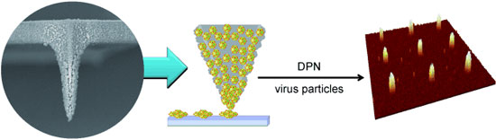
Pen-pushing: Direct-write dip-pen nanolithography (DPN) using a tip coated with nanoporous poly(2-methyl-2-oxazoline) allows the creation of precise patterns of large-sized biomaterials such as viruses. The hydrogel tip absorbs the virus-containing ink solution and atomic force microscopy is used to transport it to a surface. (Reprinted with permission from Wiley-VCH Verlag)
Focused Ion Beam Lithography (FIBL)
Focused Ion Beam Lithography (FIBL) emerged in the late 20th century as a complementary technique to Electron Beam Lithography (EBL). It uses a focused beam of ions instead of electrons or photons to create patterns in a resist or directly on a substrate.
The FIBL process begins similarly to other lithographic techniques, with a substrate coated in a resist sensitive to ion exposure. The ion beam, commonly formed from Gallium ions, is focused onto the resist, and the beam's position is controlled to draw the desired pattern. The ions interact with the resist, causing a change in its properties which allows the subsequent development process to selectively remove the exposed or unexposed regions.
What differentiates FIBL from other lithographic methods is its ability to directly mill or modify a substrate without a resist. When the ions hit the substrate, they can physically sputter away atoms from the surface, allowing direct etching of the material. The ions can also induce local chemical reactions when specific precursor gases are introduced, enabling direct deposition of materials.
The main advantage of FIBL is its versatility. Its direct-write capabilities make it an ideal tool for rapid prototyping and modifications, and it is especially useful for creating three-dimensional structures and high aspect ratio features. FIBL is also uniquely capable of both adding and removing material, which opens up possibilities for complex and precise microfabrication tasks.
However, like EBL, FIBL is a relatively slow, serial process, making it less suitable for high-volume manufacturing. The use of ion beams also introduces additional challenges. The ion-substrate interactions can cause damage to the substrate, which can be a concern for certain sensitive materials or devices. Furthermore, because ion sources typically use liquid metal ion sources, often gallium, there can be issues with contamination.
Despite these challenges, FIBL has found valuable applications in microfabrication, particularly for tasks that require the three-dimensional manipulation of materials at the nanoscale. In recent years, it has been widely used in the semiconductor industry for circuit editing and failure analysis. In the research environment, FIBL is a powerful tool for creating novel nanoscale devices and structures.
Introduction to Focused Ion Beam
Comparison of the Different Types of Lithography
Suitability for Different Applications
Each type of lithography has its unique advantages that make it suitable for different applications. Photolithography's high throughput and cost-effectiveness make it the preferred choice for large-scale manufacturing, particularly in the microelectronics industry. Similarly, EUVL, though complex and costly, is increasingly important for manufacturing the latest generation of semiconductor devices with feature sizes of 5 nm and below.
Electron Beam Lithography, despite its low throughput, offers high resolution and flexibility, making it ideal for research and prototyping, as well as for manufacturing specialized devices where small quantities are needed, such as in photonics or quantum computing.
NIL and X-ray lithography both offer high resolution, and their ability to pattern large areas in a single step makes them attractive for creating repeating patterns. NIL, in particular, has been successfully applied in microelectronics, photonics, and data storage.
Dip Pen Nanolithography is unique in its ability to directly write a wide range of materials, making it particularly suited to applications in materials science, nanotechnology, and biotechnology. Focused Ion Beam Lithography, with its capability to add and remove material, is a powerful tool for creating novel nanoscale devices and structures, particularly in a research environment.
Speed and Efficiency
Photolithography and EUVL are among the fastest lithography techniques due to their ability to pattern entire wafers in a single exposure. NIL and X-ray lithography also have relatively high throughput due to their ability to pattern large areas in one step.
On the other hand, Electron Beam, Focused Ion Beam, and Dip Pen Nanolithography are slower, serial processes. They require the beam or tip to be scanned across the surface to write each feature, making them less efficient for large-scale manufacturing.
Cost-Effectiveness
Photolithography is generally the most cost-effective lithography technique for large-scale manufacturing due to its high throughput and the extensive infrastructure already in place. NIL and X-ray lithography can also be cost-effective for certain applications due to their high throughput.
However, the high cost of equipment and infrastructure for EUVL, X-ray lithography, and FIBL can be a barrier to their adoption. DPN and EBL, while offering high resolution and flexibility, also tend to be less cost-effective due to their low throughput.
Resolution and Precision
The resolution of a lithography technique depends on the wavelength of the radiation used (for photolithography, EUVL, and X-ray lithography) or the size of the beam or tip (for EBL, FIBL, and DPN). EUVL, with its 13.5 nm wavelength, currently offers the highest resolution among commercial lithography techniques. EBL and FIBL can achieve high resolution due to the small size of the electron or ion beam, while DPN's resolution is limited by the size of the AFM tip and the spreading of the ink on the substrate.
The precision of a lithography technique depends on the stability and control of the exposure process. All of the techniques discussed here can achieve high precision, but factors such as exposure dose control, alignment accuracy, and environmental stability can influence the final precision achieved.
Frequently Asked Questions (FAQs) about Lithography
What is Lithography in Nanotechnology?
Lithography in nanotechnology is a process used to create patterns on a nanoscale, which helps in the fabrication of nanodevices and systems.
What are the types of lithography techniques in nanotechnology?
There are several types of lithography techniques in nanotechnology including Photolithography, Electron Beam Lithography, Nanoimprint Lithography, and Extreme Ultraviolet Lithography.
What is Photolithography?
Photolithography is a process that uses light to transfer geometric patterns onto a substrate to create nanoscale structures.
What is Electron Beam Lithography?
Electron Beam Lithography is a lithographic process that uses a focused beam of electrons to create patterns at the nanoscale.
How does Nanoimprint Lithography work?
Nanoimprint Lithography is a technique where a template is pressed into a resin on a substrate, creating nanoscale patterns when the resin hardens.
What is Extreme Ultraviolet Lithography?
Extreme Ultraviolet Lithography uses light of extremely short wavelength to create intricate nanostructures, often used in advanced semiconductor fabrication.
How is Lithography used in Nanotechnology?
Lithography is used to create and replicate patterns on a nanoscale, which are fundamental in the fabrication of nanodevices like microprocessors, sensors, and more.
What are the advantages of Photolithography?
Photolithography offers high throughput and cost-effectiveness, making it suitable for mass production of nanostructures.
What are the limitations of Electron Beam Lithography?
Electron Beam Lithography, while precise, can be time-consuming and expensive due to low throughput and high energy consumption.
Why is Nanoimprint Lithography important?
Nanoimprint Lithography provides high-resolution and high-throughput patterning capabilities, playing a crucial role in nanodevice fabrication.
How does Extreme Ultraviolet Lithography improve semiconductor fabrication?
Extreme Ultraviolet Lithography allows for the creation of smaller, more intricate features on semiconductors, enhancing their performance and efficiency.
What materials can be used in Nanolithography?
Various materials like silicon, germanium, gallium arsenide, polymers, and more can be patterned using nanolithography techniques.
What is the future of Lithography in Nanotechnology?
The future of lithography in nanotechnology is likely to see developments in achieving higher resolution, faster throughput, and cost-effectiveness in nanostructure fabrication.
How has Lithography shaped the field of Nanotechnology?
Lithography has enabled the development of numerous nanoscale devices and systems, profoundly influencing sectors like electronics, healthcare, energy, and more.
What industries benefit from Nanolithography techniques?
Industries like electronics, healthcare, energy, environmental science, and more benefit from the precise, scalable fabrication enabled by nanolithography techniques.
