Nanotechnology Frequently Asked Questions
This FAQ covers the most common questions about nanotechnology, from basic definitions to real-world applications and safety considerations. For a comprehensive introduction, see our Ten Things You Should Know About Nanotechnology series.
Basic Concepts
What is nanotechnology?
Major technology shifts don't happen overnight, and rarely are they the result of a single breakthrough discovery. Nowhere is this more true than for the vast set of capabilities that we have come to simply call nanotechnology.
Nanotechnology is not an industry; nor is it a single technology or a single field of research. What we call nanotechnology consists of sets of enabling technologies applicable to many traditional industries (therefore it is more appropriate to speak of nanotechnologies in the plural).
At its core, nanotechnology is the understanding and control of matter at the nanometer scale (1-100 nanometers), where unique phenomena enable novel applications. It encompasses imaging, measuring, modeling, and manipulating matter at this length scale.
What exactly is nanotechnology? We answer this question in depth in our Introduction to Nanotechnology section.
What is the difference between nanoscience and nanotechnology?
Nanoscience is the study of phenomena and manipulation of materials at the nanoscale, where properties differ significantly from those at a larger scale. It focuses on understanding the fundamental science of nanoscale systems.
Nanotechnology is the application of nanoscience to create useful materials, devices, and systems. It involves designing, characterizing, producing, and applying nanoscale structures for practical purposes.
In practice, the two terms are often used interchangeably, but nanoscience emphasizes discovery and understanding while nanotechnology emphasizes application and engineering.
How big is a nanometer?
A nanometer is one billionth of a meter. The prefix nano means 'one billionth', or 10-9, in the international system for units of weights and measures. The abbreviation for nanometer is nm. The term nanos comes from the Greek word for dwarf.
To put this in perspective:
• A human hair is about 80,000-100,000 nanometers wide
• A red blood cell is about 7,000 nanometers in diameter
• A DNA double helix is about 2 nanometers in diameter
• A single gold atom is about 0.3 nanometers across
Also check our metric prefix table.
What is so special about nanotechnology?
At the nanoscale, materials can exhibit dramatically different properties than they do in bulk form. This happens because of two main phenomena:
Surface effects: As particles get smaller, a greater proportion of atoms are on the surface rather than the interior. Since surface atoms behave differently from interior atoms, this changes the material's overall properties, including reactivity, strength, and electrical characteristics.
Quantum effects: At the nanoscale, quantum mechanical effects become significant. Electrons become confined in ways that change optical, electrical, and magnetic properties. This is why gold nanoparticles can appear red or purple instead of gold, and why quantum dots emit different colors depending on their size.
For more details, read our section on what is so special about nanotech.
How does nanotechnology work?
Nanotechnology works by manipulating matter at the atomic and molecular level to create materials and devices with novel properties. There are two main approaches:
Top-down: Starting with larger materials and reducing them to nanoscale structures. This includes techniques like lithography (used to make computer chips), milling, and etching.
Bottom-up: Building structures atom by atom or molecule by molecule. This includes self-assembly, where molecules naturally arrange themselves into ordered structures, and chemical synthesis of nanomaterials.
Modern nanotechnology often combines both approaches. For example, semiconductor manufacturing uses top-down lithography to create nanoscale patterns, while the growth of carbon nanotubes relies on bottom-up chemical processes.
Nanomaterials
What are nanomaterials?
Much of nanoscience and many nanotechnologies are concerned with producing new or enhanced materials. Nanomaterials can be constructed by top down techniques, producing very small structures from larger pieces of material, for example by etching to create circuits on the surface of a silicon microchip. They may also be constructed by bottom up techniques, atom by atom or molecule by molecule.
According to the EU definition, if 50% or more of the constituent particles of a material in the number size distribution have one or more external dimensions in the size range 1 nm to 100 nm, then the material is a nanomaterial.
Even if a product contains nanomaterials, or when it releases nanomaterials during use or ageing, the product itself is not a nanomaterial unless it is a particulate material that meets the criteria of particle size and fraction.
What are zero-, one-, two-, and three-dimensional nanomaterials?
Nanomaterials are categorized based on the number of dimensions confined to the nanoscale:
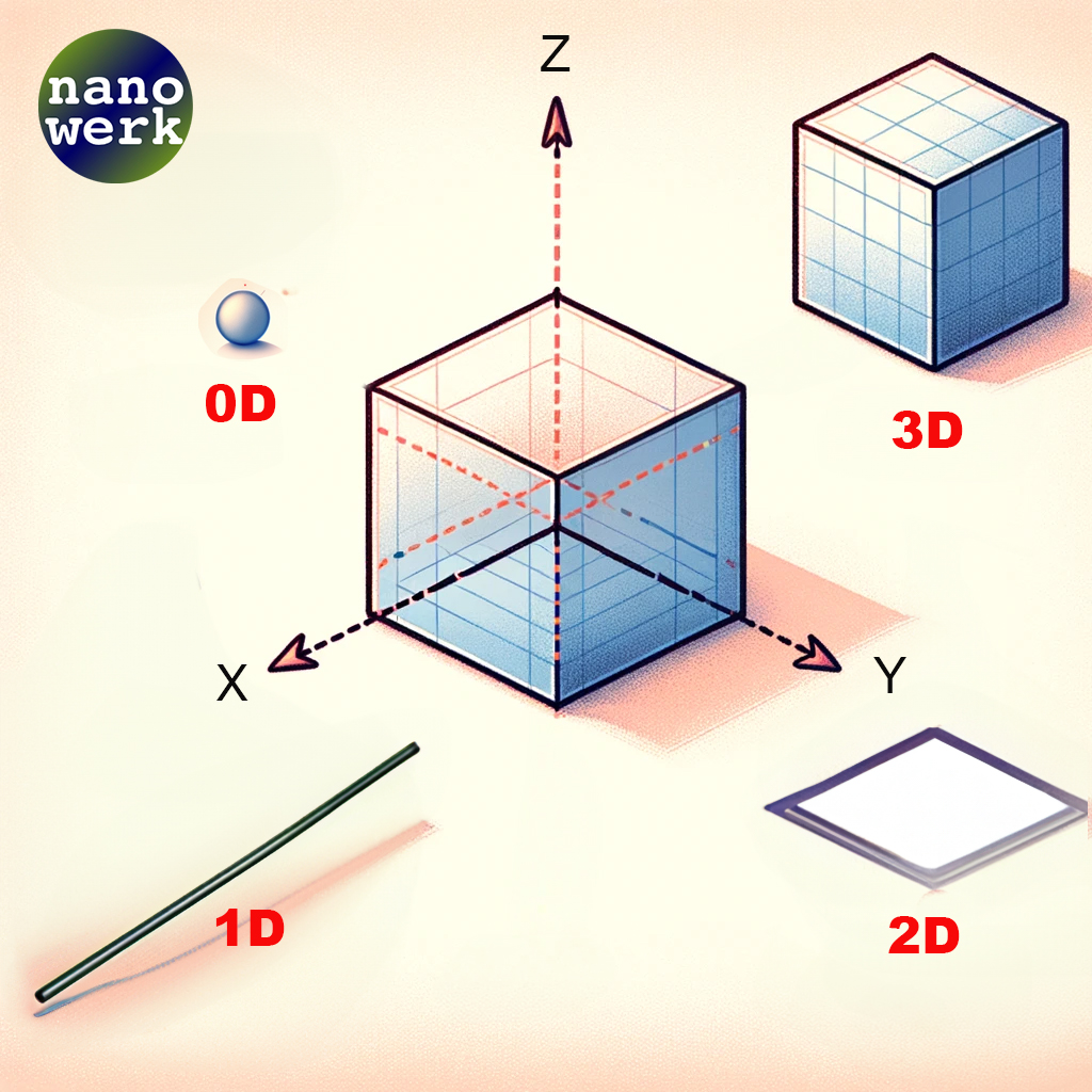
Classification of nanoscale dimensions. (© Nanowerk)
Zero-dimensional (0D): All three dimensions are confined to the nanoscale. Examples include quantum dots and nanoparticles. Electrons experience quantum confinement in all directions, leading to unique optical and electronic properties.
One-dimensional (1D): Two dimensions are confined while one extends beyond the nanoscale. Examples include nanotubes, nanorods, and nanowires. Electrons can move along the length but are confined in the other directions.
Two-dimensional (2D): One dimension is confined while two extend beyond the nanoscale. Examples include graphene, nanofilms, and nanocoatings. These ultra-thin materials have exceptional surface area and unique electrical properties.
Three-dimensional (3D): None of the dimensions are confined to the nanoscale, but the material is composed of nanoscale building blocks. Examples include bulk powders of nanoparticles and nanocomposites.
What is graphene?
Graphene is a single layer of carbon atoms arranged in a two-dimensional hexagonal lattice. It is the basic structural element of other carbon allotropes including graphite, carbon nanotubes, and fullerenes.
Graphene has remarkable properties: it is the strongest material ever tested, conducts electricity better than copper, and is nearly transparent. Its discovery led to the 2010 Nobel Prize in Physics for Andre Geim and Konstantin Novoselov.
We have a detailed article for you on what graphene is, complete with an introductory video.
What are carbon nanotubes?
Carbon nanotubes (CNTs) are cylindrical structures made of rolled-up sheets of graphene. They can be single-walled (one layer) or multi-walled (multiple concentric layers).
CNTs have extraordinary properties: they are stronger than steel, excellent conductors of electricity and heat, and extremely lightweight. Applications include composite materials, electronics, energy storage, and sensors. The 2024 Kavli Prize in Nanoscience was awarded to researchers for their foundational work on carbon nanotubes.
What are quantum dots?
Quantum dots are semiconductor nanocrystals, typically 2-10 nanometers in diameter. Their small size causes quantum confinement effects that give them unique optical properties.
The key feature of quantum dots is that their color (the wavelength of light they emit) depends on their size. Smaller dots emit blue light; larger dots emit red light. This tunability makes them valuable for displays, solar cells, and biomedical imaging. The 2023 Nobel Prize in Chemistry was awarded to Moungi Bawendi, Louis Brus, and Alexei Ekimov for their discovery and development of quantum dots.
What are synthetic nanoparticles?
Synthetic nanoparticles are engineered particles with dimensions between 1-100 nanometers, designed for specific applications. Unlike naturally occurring nanoparticles (from volcanic ash, sea spray, etc.), synthetic nanoparticles are manufactured with controlled size, shape, and surface properties.
Common types include metal nanoparticles (gold, silver), metal oxide nanoparticles (titanium dioxide, zinc oxide), and polymer nanoparticles. Applications span medicine, electronics, energy, and consumer products.
How are nanoparticles made?
Nanoparticles can be made through various methods:
Chemical synthesis: Chemical reactions in solution to precipitate nanoparticles with controlled properties.
Physical methods: Laser ablation, sputtering, or mechanical milling to break down bulk materials.
Biological methods: Using bacteria, fungi, or plant extracts to synthesize nanoparticles (green synthesis).
Vapor deposition: Condensing materials from gas phase onto substrates.
We have a detailed article for you on how nanoparticles are made.
Applications and Products
What are real-world examples of nanotechnology?
Nanotechnology is already in many everyday products:
Electronics: Smartphone and computer processors use transistors at the 3nm scale, with billions on a single chip.
Medicine: COVID-19 mRNA vaccines use lipid nanoparticles to deliver genetic material. Cancer drugs like Doxil and Abraxane use nanoparticle formulations for targeted delivery.
Consumer products: Sunscreens with zinc oxide and titanium dioxide nanoparticles; stain-resistant fabrics with nanocoatings; scratch-resistant eyeglass coatings.
Displays: Samsung QLED TVs use quantum dots for enhanced color.
Energy: Nanostructured electrodes in lithium-ion batteries; anti-reflective coatings on solar panels.
For further reading, we have compiled numerous articles on nanotechnology applications.
Where is nanotechnology used today – Can I buy nanotechnology products?
Yes! Nanotechnology has become ubiquitous in daily life. Consumers encounter nanotechnology in food packaging, textiles, cosmetics, electronics, sporting goods, and medical treatments.
Examples include: UV filters in sunscreens (titanium dioxide and zinc oxide nanoparticles); antimicrobial coatings using nanosilver; self-cleaning surfaces; improved batteries in electric vehicles; water filtration membranes; and advanced drug delivery systems.
The most visible recent example is the COVID-19 mRNA vaccines (Pfizer-BioNTech and Moderna), which use lipid nanoparticles to deliver the vaccine's genetic instructions into cells. Billions of doses have been administered worldwide.
How big is the nanotechnology market?
The global nanotechnology market is valued at approximately $80-90 billion as of 2024, with projections to reach $200-300 billion by the early 2030s.
Healthcare applications lead adoption, representing over 25% of the market. Electronics and energy are also major sectors.
Government investment remains strong: the US National Nanotechnology Initiative budget is $2.2 billion for 2025 (a record), with cumulative investment exceeding $45 billion since 2001. The EU's Horizon Europe program allocates approximately €1.3 billion for nanotechnology research.
For more details, see our page on nanotechnology market statistics, investments, and publications.
Where will nanotechnology take us?
When we ask 'where nanotechnology will take us', we need to differentiate between two types of development:
Evolutionary nanotechnology is happening now: continuously improving existing processes, materials, and applications by scaling down and exploiting nanoscale phenomena. This includes ever-smaller transistors, better batteries, more effective drug delivery, and enhanced materials.
Revolutionary nanotechnology envisions building complex systems atom by atom, including molecular machines and advanced manufacturing systems. While significant progress has been made in molecular nanotechnology, fully autonomous nanoscale machines remain largely in the research phase.
Near-term advances likely include: continued semiconductor miniaturization, personalized nanomedicine, improved energy storage and generation, advanced water treatment, and smart materials that respond to their environment.
Safety and Regulation
Is nanotechnology safe? Are there health risks from nanoproducts?
There is no simple 'yes' or 'no' answer. Safety depends on the specific nanomaterial, its properties, the application, and the exposure route.
The mere presence of nanomaterials is not inherently dangerous. Nanoparticles exist naturally in the environment. Many engineered nanomaterials have been used safely for decades (carbon black in tires, for example), and billions of mRNA vaccine doses using lipid nanoparticles have been administered safely worldwide.
However, some nanomaterials may pose risks under certain conditions. The field of nanotoxicology studies these potential effects. Key factors affecting safety include particle size, shape, surface chemistry, solubility, and whether nanoparticles are "free" (can be inhaled or absorbed) or "fixed" (embedded in a matrix).
We cover this topic comprehensively in our Nanotechnology: The Risk Factor article.
How is nanotechnology regulated?
Comprehensive regulatory frameworks now govern nanomaterials in major markets:
European Union: Nanomaterials are regulated under REACH (Registration, Evaluation, Authorisation and Restriction of Chemicals). Since 2020, companies must submit dedicated registration dossiers for nanomaterials to the European Chemicals Agency (ECHA). Additional sector-specific regulations cover cosmetics, food, biocides, and medical devices.
United States: The EPA regulates nanomaterials under the Toxic Substances Control Act (TSCA), with reporting requirements established in 2017. The FDA provides guidance for nanotechnology in food, cosmetics, and medical products.
International: The OECD Working Party on Manufactured Nanomaterials develops testing guidelines used worldwide.
Education and Careers
How to study nanotechnology? Where can I find nanotechnology degree programs?
Nanotechnology education typically builds on foundations in physics, chemistry, materials science, biology, or engineering, with specialization at the graduate level.
We have compiled a database with about 260 bachelor, master, Ph.D. and other certification nanotechnology and nanoscience degree programs from around the world.
What careers are available in nanotechnology?
Nanotechnology careers span many fields:
Research: Scientists and engineers in university, government, and industry labs working on fundamental discovery and applied development.
Industry: Positions in semiconductors, pharmaceuticals, energy, materials manufacturing, and consumer products companies.
Supporting roles: Regulatory affairs, patent law, science communication, and technical sales.
Educational backgrounds typically include physics, chemistry, materials science, electrical engineering, biomedical engineering, or chemical engineering, often with graduate degrees for research positions.
Research and Industry
Who is developing nanotechnology?
Researchers in thousands of university, industry, and government laboratories around the world. Our Nanotechnology Company & Research Laboratories Directory currently lists almost 3000 entries.
Leading research countries by publication output include China (which now produces the most nanotechnology papers), the United States, India, South Korea, and European nations including Germany, the UK, and France.
What countries are active in nanotechnology?
Nanotechnology research and development is global. China now leads in scientific publications, followed by the United States, India, and South Korea. In patents, the US leads, followed by South Korea, China, Taiwan, and Japan.
Our Global Nanotechnology Markets section lists companies, research laboratories, and degree programs by country.
Where can I find companies that make nanomaterials?
Our extensive nanotechnology company database lists raw material producers, companies in biomedicine and life sciences, product manufacturers, instrument suppliers, and service providers.
We have also compiled specialized lists for Graphene Manufacturers and Suppliers; Carbon Nanotube Manufacturers and Suppliers; and Atomic Force Microscope Manufacturers.
What professional journals cover nanotechnology?
We have compiled a global nanotech publications directory listing more than 230 academic journals dedicated wholly or primarily to nanoscience and nanotechnology, including academic journals, magazines, newsletters, and book series.
Leading journals include Nature Nanotechnology, Nano Letters, ACS Nano, Nanoscale, and Small, among many others.
Where can I find nanotechnology conferences and events?
Show me some cool nanotechnology images
Happy to! Some of the many nanotechnology images we have compiled will blow your mind. These include electron microscope images of nanomaterials, artistic renderings, and visualizations of nanoscale structures.
