Ten Things You Should Know About Nanotechnology
Part 3 of 10 | View all topics
 |
3) What's So Special About Nanotechnology? |
Nanoparticles Have Always Been Around
Chemists have dealt with naturally occurring nanoparticles all along. Think molecules or viruses. Toxicologists have dealt with nanoparticles that are the result of modern human life, such as carbon particles in combustion engine exhaust. Without being aware of it, tire manufacturers used nanoparticles (carbon black) to improve the performance of tires as early as the 1920s.
Medieval artists used gold nanoparticles to achieve the bright red color in church windows like the one shown below; gold particles at nanometer size are red, not golden. You might even say that we are surrounded by, and made of, nanostructures since atoms and molecules are nanoscale objects after all.

The north rose window of the Chartres Cathedral (Chartres, France)
So what changed? Why is nanotechnology now such an important field?
The Tools That Made It Possible
The ongoing quest for miniaturization has resulted in tools such as the atomic force microscope (AFM) and the scanning tunneling microscope (STM). Combined with refined processes such as electron beam lithography, these instruments allow the deliberate manipulation and manufacture of nanostructures ("High-speed AFM enables real-time nanofabrication"). This wasn't possible before.
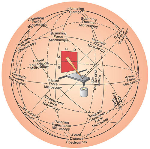
The AFM (center) has inspired a variety of other scanning probe techniques. Originally the AFM was used to image the topography of surfaces, but by modifying the tip it is possible to measure other quantities such as electric and magnetic properties, chemical potentials, and friction. (Image: Christoph Gerber)
With new tools came new concepts, and it turned out that the mechanical rules that govern the nanoworld are quite different from our everyday macroworld experience. Only a few decades ago, the possibility that one could directly measure the forces acting between molecules appeared remote. The advent of nanotechnology has dramatically changed this perception. Today there are a number of tools that can be used to characterize the nanomechanics of biomolecular and cellular interactions, including optical tweezers, magnetic pullers, and cantilever based instruments like the AFM.
Engineered nanomaterials, either by way of a top-down approach (a bulk material is reduced in size to nanoscale patterns) or a bottom-up approach (larger structures are built atom by atom or molecule by molecule), go beyond just a further step in miniaturization. For a discussion on nanotechnology top-down versus bottom-up see part 5 "Nanomanufacturing" of this section.
Quantum Effects
The bulk properties of materials often change dramatically when reduced to nanoscale dimensions. Starting roughly at 100 nanometers and below, materials break a size barrier below which quantization of energy for the electrons in solids becomes relevant.
The quantum size effect describes the physics of electron properties in solids with great reductions in particle size. This effect does not come into play by going from macro to micro dimensions. However, it becomes dominant when the nanometer size range is reached.
Quantum effects can begin to dominate the behavior of matter at the nanoscale, particularly at the lower end (single digit and low tens of nanometers), affecting the optical, electrical and magnetic behavior of materials. Materials can be produced that are nanoscale in one dimension (for example, very thin surface coatings), in two dimensions (for example, nanowires and nanotubes) or in all three dimensions (for example, nanoparticles and quantum dots).
The causes of these drastic changes stem from the world of quantum physics. The bulk properties of any material are merely the average of all the quantum forces affecting all the atoms that make up the material. As you make things smaller and smaller, you eventually reach a point where the averaging no longer works and you have to deal with the specific behavior of individual atoms or molecules, behavior that can be very different from when these atoms are aggregated into a bulk material.
Materials reduced to the nanoscale can suddenly show very different properties compared to what they show on a macroscale. For instance, opaque substances become transparent (copper); inert materials become catalysts (platinum); stable materials turn combustible (aluminum); solids turn into liquids at room temperature (gold); insulators become conductors (silicon).
Surface Area
Another important aspect of nanomaterials is surface area. When compared to the same mass of material in bulk form, nanoscale materials have a relatively larger surface area. This can make materials more chemically reactive (in some cases materials that are inert in bulk form are reactive when produced in their nanoscale form), and affect their strength or electrical properties.

To understand the effect of particle size on surface area, consider an American Silver Eagle coin. This silver dollar contains 31 grams of coin silver and has a total surface area of approximately 3000 square millimeters. If the same amount of coin silver were divided into tiny particles, say 10 nanometers in diameter, the total surface area of those particles would be 7000 square meters (equal to the size of a soccer field, or larger than the floor space of the White House at 5100 square meters). In other words: when the amount of coin silver contained in a silver dollar is rendered into 10 nm particles, the surface area of those particles is over 2 million times greater than the surface area of the silver dollar.
The fascination with nanotechnology stems from these unique quantum and surface phenomena that matter exhibits at the nanoscale, making possible novel applications and interesting materials.
Evolutionary vs. Revolutionary Nanotechnologies
There is a need to differentiate between two types of nanotechnologies. One is happening right now and the other remains the stuff of science fiction and speculative technology scenarios.
What we are dealing with today is evolutionary nanotechnology. The goal is to improve existing processes, materials and applications by scaling down into the nano realm and ultimately exploiting the unique quantum and surface phenomena that matter exhibits at the nanoscale. This trend is driven by companies' ongoing quest to improve existing products by creating smaller components and better performance materials, all at a lower cost.
The semiconductor industry provides the clearest example. Chip design structures broke the 100 nanometer barrier years ago, and the industry has been a nanotechnology industry ever since.


Left: the first point contact transistor built in 1947. Right: modern chips contain billions of transistors, each just a few nanometers in size.
The first transistors were over 1 centimeter in size. Today's most advanced transistors are just 3 nanometers or smaller, over three million times smaller than those first devices. TSMC and Samsung are already manufacturing at 3nm nodes, with 2nm production on the horizon. This feat is equivalent to shrinking a tall skyscraper to the size of a grain of rice. When we reach single molecule transistors, it will mark the end of a gradual miniaturization that began in 1947.
Due to this continuing trend of "smaller, better, cheaper," the number of companies that are, by definition, "nanotechnology companies" (because they use nanoformulated ingredients, nanoparticle coatings, nanostructured surfaces, or carbon nanotube based electronics) continues to grow rapidly across many industries.
By contrast, truly revolutionary nanotechnology envisions a bottom-up approach where functional devices and entire fabrication systems are built atom by atom. Here we are not just talking about self-assembly and chemical synthesis of nanomaterials but functional machinery. Unless you resort to science fiction scenarios, it remains impossible to make educated guesses as to what that future might bring.
Now that we understand what makes nanotechnology special, let's look at one of its most exciting areas: the rise of carbon nanomaterials.
