What Is Graphene? Properties, Production, and Uses
Table of Contents
- 1. What is graphene – Properties and structure
- 2. Graphene oxide: Uses, production, and differences from graphene
- 3. Other forms of graphene – graphdiyne and holey graphene
- 4. The fascinating story of graphene's discovery
- 5. Graphene production methods: A comprehensive guide
- 6. Overcoming the challenges of graphene manufacturing
- 7. Graphene properties
- 8. Graphene's potential: Revolutionizing industries
- 9. Frequently Asked Questions (FAQs)
Graphene is a single layer of carbon atoms arranged in a hexagonal lattice structure, forming a two-dimensional (2D) material with exceptional mechanical, electrical, and thermal properties. It is widely studied for its potential use in various fields such as electronics, energy storage, and biomedicine.
Graphene has emerged as one of the most promising nanomaterials because of its unique combination of exceptional properties: it is not only the thinnest but also one of the strongest materials; it conducts heat better than all other materials; it is an excellent conductor of electricity; it is optically transparent, yet so dense that it is impermeable to gases – not even helium, the smallest gas atom, can pass through it.
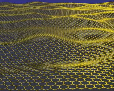 Graphene – the mother of all graphitic forms. Shown on the left is an artistic impression of a corrugated graphene sheet (Image: Jannik Meyer).Graphene's unique combination of extraordinary properties offers a fascinating material platform for the development of next-generation technologies in many areas – wearable and superfast electronics, ultrasensitive sensors, multifunctional composites and coatings, membranes, medicine and biotechnology, energy harvesting and storage.
Since its isolation in 2004, graphene research has expanded into a massive interdisciplinary field, now yielding approximately 30,000 scientific papers annually across a vast range of applications.
Key Takeaways About Graphene
- What it is: A single-atom-thick layer of carbon arranged in a hexagonal lattice – the thinnest material known
- Key properties: 200× stronger than steel, excellent electrical and thermal conductor, flexible, transparent, and impermeable to gases
- Production methods: Mechanical exfoliation, chemical vapor deposition (CVD), and reduction of graphene oxide
- Major applications: Electronics, energy storage, biomedicine, composites, sensors, and water filtration
- Current challenges: Mass production with consistent quality, integration with existing technologies, and cost-effectiveness
- Future outlook: Expected to revolutionize multiple industries by 2030 and beyond, with growing commercial adoption in batteries, electronics, and composite materials
What is graphene – Properties and structure
Graphene is a single layer — or monolayer — of carbon atoms bonded together in a repeating hexagonal pattern. This sheet is only one atom thick. When many graphene layers are stacked on top of one another, they form graphite, the familiar material used in pencil “lead.” The spacing between graphene layers in graphite is about 0.335 nanometers, which means that a 1 mm thick sheet of graphite contains roughly 3 million graphene layers.

In scientific terms, graphene’s unusual behavior comes from the bonding of carbon atoms in an atom-thin honeycomb lattice. Each carbon atom forms strong in-plane bonds with its three neighbors, while its remaining electron contributes to delocalized π-bands that extend across the sheet. This electronic structure is responsible for many of graphene’s remarkable electrical, optical, thermal, and mechanical properties.
Pristine monolayer graphene is among the strongest materials ever measured. Its intrinsic tensile strength is about 130 GPa, and its stiffness is around 1 TPa — far higher than steel on a strength-to-weight basis. At the same time, because it is only one atom thick, graphene can bend and flex without the bulkiness of conventional materials.
To put this in perspective: in an idealized comparison, if a sheet of kitchen cling film had the same intrinsic strength as pristine monolayer graphene, puncturing it with a pencil would require a force comparable to the weight of a large car — roughly equivalent to a 2,000 kg mass. This comparison assumes a perfect, defect-free graphene sheet; real graphene materials can be much weaker depending on defects, grain boundaries, layer number, and processing quality.
Graphene’s structure also gives it an unusual combination of other properties. Under ideal conditions, its electron mobility can be up to about 100 times higher than silicon; its thermal conductivity can reach roughly 2,000–5,000 W/m·K, comparable to or higher than diamond; a single layer absorbs only about 2.3% of incident visible light, making it nearly transparent; and a defect-free monolayer is impermeable even to helium atoms.
Graphene also has a theoretical specific surface area of about 2,630 m²/g when both sides of the sheet are accessible. Since that value counts both sides, about 6 grams of ideal monolayer graphene would provide enough one-sided area to cover a full-size soccer field, though practical materials usually provide less accessible surface area because sheets can overlap, wrinkle, fold, or restack.
Graphene is part of a conceptually new class of atomically thin materials known as two-dimensional, or 2D, materials. They are called 2D because they extend mainly in length and width, while their thickness is only one or a few atoms. Many of graphene’s most extraordinary properties are strongest in pristine single-layer or few-layer form and may change substantially in bulk graphite, multilayer films, powders, flakes, coatings, or composites.
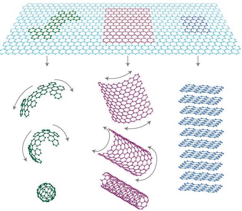
Graphene is the basic building block for other graphitic materials like carbon nanotubes:
Graphene oxide: Uses, production, and differences from graphene
Graphene oxide (GO) is a single atom carbon layer where both surfaces of the layer are modified by oxygen containing functional groups. In multi-layer graphene oxide, the carbon layers are separated by functional groups bonded to each layer of carbon atoms.
Although GO – like graphene – is a 2D material, its properties are very different from that of graphene. It does not absorb visible light, has very low electric conductance compared to that of graphene, and demonstrates significantly higher chemical activity.
Graphene oxide was discovered more or less by accident by British chemist Benjamin Brodie in 1859. In his experiments, he exposed graphite to strong acids and obtained what he called carbonic acid. Brodie believed that he discovered graphon, a new form of carbon with a molecular weight of 33.
As Andre Geim writes in his article on Graphene Prehistory, "Today we know that he observed a suspension of tiny crystals of graphene oxide, that is, a graphene sheet densely covered with hydroxyl and epoxide groups."
At the beginning of the wave of interest GO was considered only as the way for mass production of cheap graphene, in particular the preparation of single and multilayer graphene films and bulk graphene structures by reduction (resulting in reduced graphene oxide, or rGO).
Over time, as we show in some of the examples below, GO has found applications in many areas such as membranes, coatings, sensors, photocatalysis, and solar cells. And although GO, and its reduced form rGO, is the closest relative of graphene, owing to its unique properties it has established its own independent place in the graphene family.
Other forms of graphene – graphdiyne and holey graphene
The main challenge of using graphene in electronics is the zero-bandgap electronic structure of graphene. This makes it impossible to switch off graphene-based transistors, which limits their application in the semiconductor industry.
While it is possible to overcome this limitation by doping or functionalizing the graphene, there is also much interest in the search for new types of 2D carbon allotropes that have exceptional semiconducting properties, such as a proper energy bandgap and high mobility.
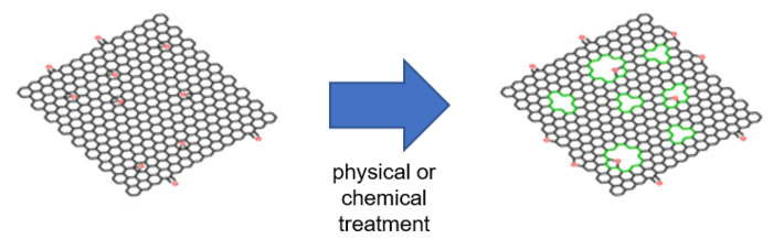
Researchers discovered that it is possible to endow many characteristics suitable for a semiconductor to graphene or graphene oxides by creating many holes in its structure. This new type of material is called 'holey graphene'. Compared to graphene, γ-graphyne, or graphdiyne, holey graphene not only has the ideal 2D semiconducting properties but also has nonlinear sp bonding and a special π-conjugated structure, which offers promising applications in optoelectronic, energy harvesting, gas separation, catalysis, water remediation, sensor, and energy-related fields.
The fascinating story of graphene's discovery
Before graphene was first demonstrated in 2004 by Andre Geim and Konstantin Novoselov, two physicists from the University of Manchester, (for which they received the Nobel Prize in 2010) scientists argued that strictly 2D crystalline materials were thermodynamically unstable and could not exist.
Graphene had already been studied theoretically in 1947 by P.R. Wallace as a text book example for calculations in solid state physics. He predicted the electronic structure and noted the linear dispersion relation. The wave equation for excitations was written down by J.W. McClure already in 1956, and the similarity to the Dirac equation was discussed by G.W. Semenoff in 1984.
In 2002, Geim became interested in graphene and challenged a PhD student to polish a hunk of graphite to as few layers as possible. He managed to produce a flake of graphite roughly 1,000 layers thick - a little short of the mark.
Using a different approach, Geim’s team began to use regular scotch tape to peel away layers of graphene from a piece of graphite such as is found in ordinary pencils. Using regular adhesive tape, they ultimately managed to obtain a flake of carbon with a thickness of just one atom.
The separate layers of graphene in graphite are held together by van der Waals forces, which can be overcome during exfoliation of graphene from graphite. This mechanical peeling is the simplest of the preparation methods and surprisingly is the method that made stand-alone graphene a reality.
Since those first tiny flakes made with tape, graphene production has improved at a rapid pace. Only five years later, in 2009, researchers were able to create a graphene film that measured 30 inches across.
"Owing to its unusual electronic spectrum, graphene has led to the emergence of a new paradigm of 'relativistic' condensed-matter physics, where quantum relativistic phenomena, some of which are unobservable in high-energy physics, can now be mimicked and tested in table-top experiments," Prof. Konstantin Novoselov explained to Nanowerk back in 2007. "More generally, graphene represents a conceptually new class of materials that are only one atom thick, and, on this basis, offers new inroads into low-dimensional physics that has never ceased to surprise and continues to provide a fertile ground for applications."
"Given that graphene flakes were experimentally demonstrated in 2004 and a vast body of scientific research has been accumulated since, what happened to the promised applications of graphene and related 2D materials" you ask? Well, two 2021 publications ("Graphene Roadmap Briefs (No. 1): Innovation interfaces of the Graphene Flagship" and "Graphene Roadmap Briefs (No. 2): Industrialization status and prospects 2020") review the latest outcomes of the Graphene Technology and Innovation Roadmap, a process that explores the different pathways towards industrialization and commercialization of graphene and related materials.
The graphene community expects that, by strengthening standards and creating tailored high-quality materials, graphene materials will go beyond niche products and spearhead applications to broad market penetration by 2030. Then, graphene could be incorporated in ubiquitous commodities such as tires, batteries, sensor and electronics.
Graphene production methods: A comprehensive guide
Commercial graphene producers employ various pathways of how to make graphene. Bottom-up methods mostly rely on chemical vapor-phase deposition (CVD) of carbon-rich compounds to form 2D sheets of carbon. The obtained quality of bottom-up graphene is typically high. Unfortunately, these methods are not easily scalable and expensive.
In contrast, top-down methods are much cheaper and more scalable techniques. Many larger scale synthesis routes involve intermediate steps of graphene oxide (GO) exfoliation and subsequent reduction to reduced graphene oxide (rGO). Yet the good results obtained in terms of yield come at the cost of quality and consistency.
Currently, the most common techniques available for the production of graphene are shown schematically below, which include micromechanical cleavage, CVD, epitaxial growth on silicon carbide (SiC) substrates, chemical reduction of exfoliated graphene oxide, liquid phase exfoliation (LPE) of graphite and unzipping of carbon nanotubes.
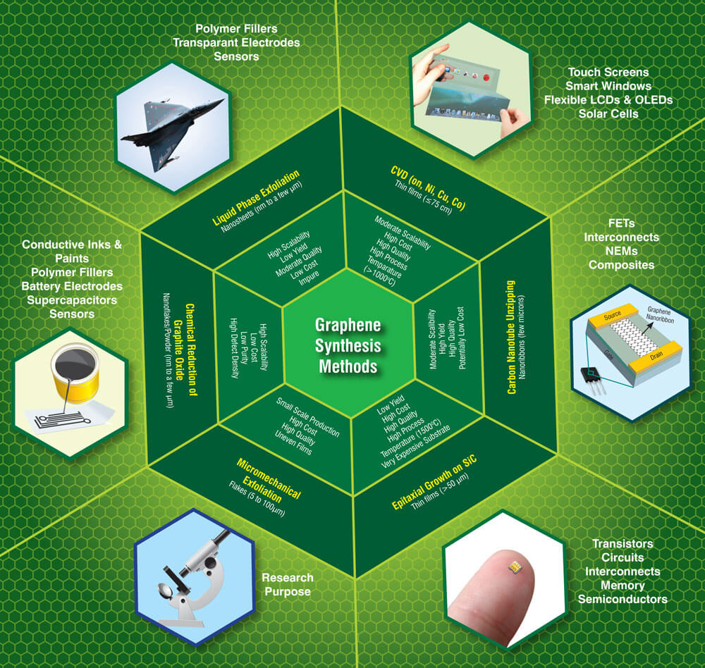
However, each of these methods can have its own advantages as well as limitations depending on its target application(s). In order to surmount these barriers in commercializing graphene, concerted efforts are being made by researchers at various R&D institutes, universities and companies from all over the globe to develop new methods for large scale production of low-cost and high-quality graphene via simple and eco-friendly approaches.
Already, researchers have managed to produce large, single-crystal-like graphene films more than a foot long on virtually any flat surface – a step towards commercialization.
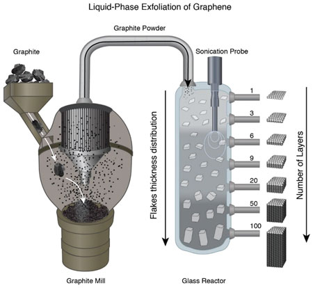
Liquid Phase Exfoliation
Among the established methods for commercial graphene production, LPE of graphite is one of the methods used most frequently. The mechanism behind LPE is based on the fact that graphite is a layered material and essentially can be seen as individual graphene crystals stacked one on top of each other.
The LPE process involves milling graphite into a powder and separating the particles into tiny flakes by applying mechanical forces in a liquid. The graphene-containing flakes are then separated from the remaining material.
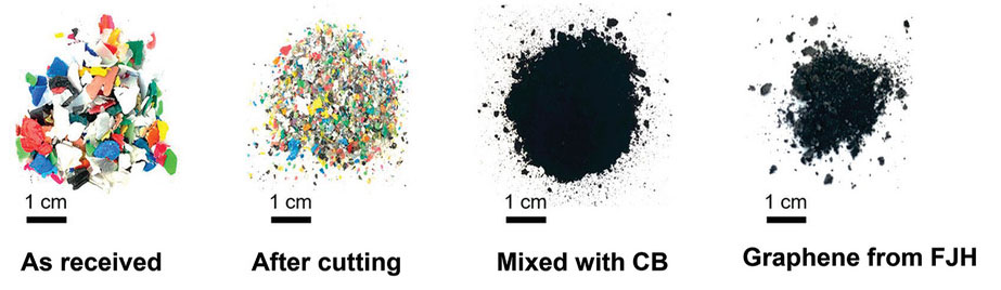
Flash Joule Heating
Flash Joule Heating (FJH) – using an electrical charge to dramatically raise a material's temperature to more than 3000 K – has been known in the literature for many decades but was more recently applied to the synthesis of graphene and other 2D materials.
In 2020, FJH was used to synthesize gram-scale quantities of graphene from a variety of feedstocks including carbon black, coal, petroleum coke, waste foods, and plastics ("Turning trash into valuable graphene in a flash").
For instance, FJH results in carbonization of mixed waste plastic and allows for direct conversion of waste plastic into graphene, without any intermediate pyrolysis processing. Since the heat necessary is generated in situ, there is no need for furnaces or inefficient heat transfer.
Read more about the large-scale synthesis of graphene and other 2D materials.
Overcoming the challenges of graphene manufacturing
Graphene has a vast number of potential applications, but research and commercial applications are undermined by the poor or unknown quality of much of the available material (read more in our article "Beware the fake graphene").
The quality of graphene plays a crucial role as the presence of defects, impurities, grain boundaries, multiple domains, structural disorders, wrinkles in the graphene sheet can have an adverse effect on its electronic and optical properties.
In electronic applications, the major bottleneck is the requirement of large size samples, which is possible only in the case of CVD process, but it is difficult to produce high quality and single crystalline graphene thin films possessing very high electrical and thermal conductivities along with excellent optical transparency.
Another issue of concern in the synthesis of graphene by conventional methods involves the use of toxic chemicals and these methods usually result in the generation hazardous waste and poisonous gases. Therefore, there is a need to develop green methods to produce graphene by following environmentally friendly approaches.
The preparation methods for graphene should also allow for in situ fabrication and integration of graphene-based devices with complex architecture that would enable eliminating the multi-step and laborious fabrication methods at a lower production cost (read more: "Mass production of high quality graphene: An analysis of worldwide patents").
Here on Nanowerk we keep an updated list of graphene manufacturers and suppliers and in our Nanowerk Product Catalog we have a list of well over 600 commercial graphene materials for sale.
Graphene properties
Electronic properties of graphene
One of the reasons nanotechnology researchers working towards molecular electronics are so excited about graphene is its electronic properties – it is one of the best electrical conductors on Earth. The unique atomic arrangement of the carbon atoms in graphene allows its electrons to easily travel at extremely high velocity without the significant chance of scattering, saving precious energy typically lost in other conductors.
Scientists have found that graphene remains capable of conducting electricity even at the limit of nominally zero carrier concentration because the electrons don't seem to slow down or localize. The electrons moving around carbon atoms interact with the periodic potential of graphene's honeycomb lattice, which gives rise to new quasiparticles that have lost their mass, or rest mass (so-called massless Dirac fermions). That means that graphene never stops conducting. It was also found that they travel far faster than electrons in other semiconductors.
Mechanical properties of graphene
The impressive intrinsic mechanical properties of graphene, its stiffness, strength and toughness, are one of the reasons that make graphene stand out both as an individual material and as a reinforcing agent in graphene composites. They are caused by the stability of the sp2 bonds that form the hexagonal lattice and oppose a variety of in-plane deformations.
A detailed discussion of the mechanical properties of graphene and graphene-based nanocomposites can be found in this review paper.
Stiffness
The breaking force obtained experimentally and from simulation was almost identical and the experimental value of the second order elastic stiffness was equal to 340 ± 50 N m-1. This value corresponds to a Young's modulus of 1.0 ± 0.1 TPa, assuming an effective thickness of 0.335 nm.
Strength
Defect-free, monolayer graphene is considered to be the strongest material ever tested with a strength of 42 N m-1, which equates to an intrinsic strength of 130 GPa.
Toughness
Fracture toughness, which is a property very relevant to engineering applications, is one of the most important mechanical properties of graphene and was measured as a critical stress intensity factor of 4.0 ±0.6 MPa.
Research groups worldwide are working on the development of industrially manufacturable graphene sheets that have high strength and toughness in all sheet directions for diverse applications as graphene-based composites for vehicles, optoelectronics and neural implants.
A recent consumer product example that exploits graphene's mechanical properties is the Momo Evo Graphene motorcycle helmet, developed by Italy's Momodesign and the Istituto Italiano di Tecnologia (IIT).
 It is the first-ever graphene-infused carbon fiber helmet that capitalizes on the material's thin, strong and conductive, flexible and light characteristics to create a helmet that absorbs and dissipates impact better than your average helmet. It also disperses heat more efficiently, so it's cooler.
Another example is the Dassi Interceptor™ Graphene bike – the world's first graphene bicycle. Enhancing carbon fiber with graphene allows to make lighter, thinner tubes, that are stronger than regular carbon. That means an aero-shaped frame with none of the usual weight sacrifice. Thanks to its graphene reinforced frame, this bike is 30% lighter yet twice as strong and super stiff.
Graphene's potential: Revolutionizing industries from electronics to medicine
Energy storage and solar cells
Graphene-based nanomaterials have many promising applications in energy-related areas. Just some recent examples: Graphene improves both energy capacity and charge rate in rechargeable batteries; activated graphene makes superior supercapacitors for energy storage; graphene electrodes may lead to a promising approach for making solar cells that are inexpensive, lightweight and flexible; and multifunctional graphene mats are promising substrates for catalytic systems.
Researchers also have discovered a critical and unexpected relationship between the graphene's chemical/structural defectiveness as a host material for electrodes and its ability to suppress the growth of dendrites – branch-like filament deposits on the electrodes that can penetrate the barrier between the two halves of the battery and potentially cause electrical shorts, overheating and fires ("Defect-free graphene might solve lithium-metal batteries' dendrite problem").
These examples highlight the four major energy-related areas where graphene will have an impact: solar cells, supercapacitors, graphene batteries, and catalysis for fuel cells.
Due to their excellent electron-transport properties and extremely high carrier mobility, graphene and other other direct bandgap monolayer materials such as transition-metal dichalcogenides (TMDCs) and black phosphorus show great potential to be used for low-cost, flexible, and highly efficient photovoltaic devices. They are the most promising materials for advanced solar cells.
An excellent review paper ("Chemical Approaches toward Graphene-Based Nanomaterials and their Applications in Energy-Related Areas") gives a brief overview of the recent research concerning chemical and thermal approaches toward the production of well-defined graphene-based nanomaterials and their applications in energy-related areas.
The authors note, however, that before graphene-based nanomaterials and devices find widespread commercial use, two important problems have to be solved: one is the preparation of graphene-based nanomaterials with well-defined structures, and the other is the controllable fabrication of these materials into functional devices.
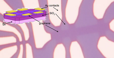
Graphene sensor applications
Functionalized graphene holds exceptional promise for biological and chemical sensors. Already, researchers have shown that the distinctive 2D structure of graphene oxide (GO), combined with its superpermeability to water molecules, leads to sensing devices with an unprecedented speed ("Ultrafast graphene sensor monitors your breath while you speak").
Scientists have found that chemical vapors change the noise spectra of graphene transistors, allowing them to perform selective gas sensing for many vapors with a single device made of pristine graphene – no functionalization of the graphene surface required ("Selective gas sensing with pristine graphene").
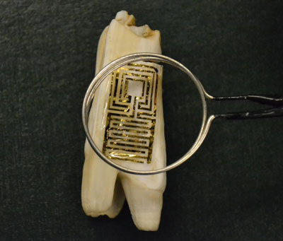
Quite a cool approach is to interface passive, wireless graphene nanosensors onto biomaterials via silk bioresorption as demonstrated by a graphene nanosensor tattoo on teeth monitors bacteria in your mouth.
Researchers also have begun to work with graphene foams – three-dimensional structures of interconnected graphene sheets with extremely high conductivity. These structures are very promising as gas sensors ("Graphene foam detects explosives, emissions better than today's gas sensors") and as biosensors to detect diseases (see for instance: "Nanotechnology biosensor to detect biomarkers for Parkinson's disease").
Graphene membranes
The us e of graphene membranes is manifold, ranging from water filtration, for instance for desalination purposes; industrial gas separation, such as CO2 capture; large-scale energy storage systems (separator membranes for redox flow batteries); or as filtration membrane in the food industry (for instance for filtering lactose from milk).
Nanofluidic membranes based on 2D materials are promising materials for next-generation water desalination and purification. For instance, pristine and chemically modified graphene oxide membranes (GOMs) effectively block organic dyes and nanoparticles as small as 9 Å. Researchers have already demonstrated a novel desalination method with nearly perfect salt rejection and high water flux.
Graphene membranes are also proposed for carbon capture, i.e., removing CO2 from emissions to prevent it from entering the atmosphere. Currently this is done by high-performance membranes made from polymers that can specifically pick out CO2 from a mix of gases. A proposed new class of high-performance membranes exceeds post-combustion capture targets by a significant margin. These membranes are based on single-layer graphene with a selective layer thinner than 20 nm and are highly tunable in terms of chemistry.
Monolayer graphene is also proposed for industrial gas separation. Separating mixed gases, such as air, into their individual components is a process with multiple industrial applications, including biogas production, air enrichment in metal working, removal of toxic gases from natural gas, and hydrogen recovery from ammonia plants and oil refineries.
However, progress with developing graphene has met with two bottlenecks: First, a lack of methods for incorporating molecular-sized pores into the layer of graphene, and second, a lack of methods for actually manufacturing mechanically robust, crack- and tear-free, large-area membranes.
In a breakthrough that solves both problems, scientists developed a large-area, single-layer graphene membrane that can separate hydrogen from methane with a high-efficiency (separation factor up to 25), and an unprecedented hydrogen permeance from a porosity that was only 0.025%.
Not a membrane application, but highly relevant for water filtration, relatively new method of purifying brackish water is capacitive deionization (CDI) technology. The advantages of CDI are that it has no secondary pollution, is cost-effective and energy efficient. Researchers have developed a CDI application that uses graphene-like nanoflakes as electrodes for capacitive deionization. They found that the graphene electrodes resulted in a better CDI performance than the conventionally used activated carbon materials ("Water desalination with graphene").
Biomedical uses of graphene
Graphene is only recently finding its way into biomedical applications. Most of the recent work in this area focuses on using graphene as a biosensor, i.e., as a passive medium, which monitors some external stimulus, usually by taking advantage of the fact that graphene's resistance depends strongly on nearby electric fields and signals (see for instance: "Graphene-DNA biosensor selective, simple to create"). But this is from a fundamental point of view nothing new; silicon wires, diamond films and carbon nanotubes all have been already used for this type of application.
Emerging uses are in stem cell therapies where graphene is used as biocompatible scaffold that does not hamper the proliferation of human mesenchymal stem cells (hMSCs) and accelerates their specific differentiation into bone cells.
The use of graphene-based materials in pharmaceutical nanotechnology has recently received more attention due to their unique chemical structure and physicochemical properties—including an ultra-high surface area, optical, thermal and electrical conductivities, and a good biocompatibility.
GO nanosheets tend to be hydrophilic and the surface contains reactive groups for an increased functionality or for loading drugs through covalent and non-covalent interactions. In addition, graphene-based nanomaterials can also be functionalized with diagnostic probes that have fluorescent and/or luminescent properties and can target ligands such as proteins, peptides, nucleic acids, antibodies, lipids, carbohydrates and folic acid.
In pharmaceutical applications, graphene-based nanomaterials possess a lot of potential for improving drug circulation times, in target drug and gene delivery systems, for acting as therapeutic agents and diagnostic tools, as well as graphene nanotheranostic agents that combine both diagnostic and therapy approaches in a single system.
An international team of researchers has developed a drug delivery technique that utilizes graphene strips as “flying carpets” to deliver two anticancer drugs sequentially to cancer cells, with each drug targeting the distinct part of the cell where it will be most effective. The technique was found to perform better than either drug in isolation when tested in a mouse model targeting a human lung cancer tumor.
Recent research also points to an opportunity to replacing antibiotics with graphene-based photothermal agents to trap and kill bacteria.
In the decades-old quest to build artificial muscles, many materials have been investigated with regard to their suitability for actuator application (actuation is the ability of a material to reversibly change dimensions under the influence of various stimuli). Besides artificial muscles, potential applications include microelectromechanical systems (MEMS), biomimetic micro-and nanorobots, and micro fluidic devices. In experiments, scientists have shown that graphene nanoribbons can provide actuation.
Graphene ink
Graphene has a unique combination of properties that is ideal for next-generation electronics, including mechanical flexibility, high electrical conductivity, and chemical stability. Numerous research efforts already have demonstrated the feasibility of fabricating graphene-based electronics through high-throughput ink printing strategies. Formulating inkjet-printable graphene ink leads to an inexpensive and scalable path for exploiting graphene's properties in real-world technologies (read more here: "Inkjet printing of graphene for flexible electronics" and here: "Direct writing with highly conductive graphene inks").
Transistors and memory
Some of the most promising applications of graphene are in electronics (as transistors and interconnects), detectors (as sensor elements) and thermal management (as lateral heat spreaders). The first graphene field-effect transistors (FETs) – with both bottom and top gates – have already been demonstrated. At the same time, for any transistor to be useful for analog communication or digital applications, the level of the electronic low-frequency noise has to be decreased to an acceptable level ("Graphene transistors can work without much noise").
Transistors on the basis of graphene are considered to be potential successors for the some silicon components currently in use. Due to the fact that an electron can move faster through graphene than through silicon, the material shows potential to enable terahertz computing.
In the ultimate nanoscale transistor – dubbed a ballistic transistor – the electrons avoid collisions, i.e. there is a virtually unimpeded flow of current. Ballistic conduction would enable incredibly fast switching devices. Graphene has the potential to enable ballistic transistors at room temperature.
While graphene has the potential to revolutionize electronics and replace the currently used silicon materials ("High-performance graphene transistor with high room-temperature mobility"), it does have an Achilles heel: pristine graphene is semi-metallic and lacks the necessary band gap to serve as a transistor. Therefore it is necessary to engineer band gaps in graphene.
Experiments have demonstrated the benefits of graphene as a platform for flash memory which show the potential to exceed the performance of current flash memory technology by utilizing the intrinsic properties of graphene.
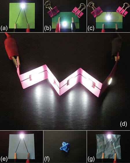
Flexible, stretchable and foldable electronics
Flexible electronics relies on bendable substrates and truly foldable electronics requires a foldable substrate with a very stable conductor that can withstand folding (i.e. an edge in the substrate at the point of the fold, which develops creases, and the deformation remains even after unfolding).
That means that, in addition to a foldable substrate like paper, the conductor that is deposited on this substrate also needs to be foldable. To that end, researchers have demonstrated a fabrication process for foldable graphene circuits based on paper substrates.
Graphene's remarkable conductivity, strength and elasticity has also made it a promising choice for stretchable electronics – a technology that aims to produce circuits on flexible plastic substrates for applications like bendable solar cells or robotic-like artificial skin.
Scientists have devised a chemical vapor deposition (CVD) method for turning graphene sheets into porous three-dimensional foams with extremely high conductivity. By permeating this foam with a siloxane-based polymer, the researchers have produced a graphene composite that can be twisted, stretched and bent without harming its electrical or mechanical properties ("Graphene: Foaming for stretchable electronics").
Photodetectors
Researchers have demonstrated that graphene can be used for telecommunications applications and that its weak and universal optical response might be turned into advantages for ultrafast photonics applications. They also found that graphene could be potentially exploited as a saturable absorber with wide optical response ranging from ultra-violet, visible, infrared to terahertz ("The rise of graphene in ultra-fast photonics").
There is a very strong research interest in using graphene for applications in optoelectronics. Graphene-based photodetectors have been realized before and graphene's suitability for high bandwidth photodetection has been demonstrated in a 10 GBit/s optical data link ("Graphene photodetectors for high-speed optical communications").
One novel approach is based on the integration of graphene into an optical microcavity. The increased electric field amplitude inside the cavity causes more energy to be absorbed, leading to a significant increase of the photoresponse ("Microcavity vastly enhances photoresponse of graphene photodetectors").
Coatings
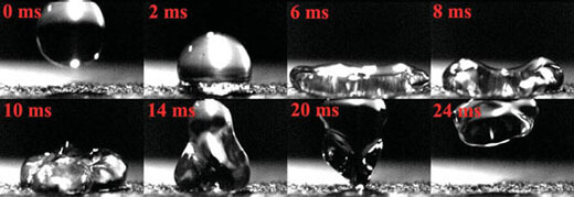
Coating objects with graphene can serve different purposes. For instance, researchers have now shown that it is possible to use graphene sheets to create a superhydrophobic coating material that shows stable superhydrophobicity under both static as well as dynamic (droplet impact) conditions, thereby forming extremely water repelling structures.
Graphene also is the world's thinnest known coating for protecting metals against corrosion. It was found that graphene, whether made directly on copper or nickel or transferred onto another metal, provides protection against corrosion.
Researchers demonstrated the use of graphene as a transparent conductive coating for photonic devices and show that its high transparency and low resistivity make this two-dimensional crystal ideally suitable for electrodes in liquid crystal devices (LCDs).
Another novel coating application useful for researchers is the the fabrication of polymeric AFM probes covered by monolayer graphene to improving AFM probe performance.
Direct laser-writing of graphene on Kevlar makes protective clothing 'smart'. Kevlar is a well-known high-strength polymer that, thanks to its excellent mechanical performance, has found a variety of important security applications especially in textiles (e.g. bullet-proof vests or firefighters' protective clothing). Get ready for the next generation of protective clothing to become multi-functional, i.e. 'smart'. These materials will not only be able to protect the human body from injury but also possess intelligent functions such as monitoring physiological signals and detecting potential hazard such as gases, pathogens, or radiation.
Van der Waals heterostructures
Graphene is also very attractive for the fabrication of mixed-dimensional van der Waals heterostructures that could be carried out through hybridizing graphene with 0D quantum dots or nanoparticles, 1D nanostructures such as nanowires or carbon nanotubes, or 3D bulk materials.
Other uses
Loudspeakers
 The extraordinary electrical and mechanical properties of graphene have been exploited to create a very efficient electrical/sound transducer. This experimental graphene loudspeaker, without any optimized acoustic design, is simple to make and already performs comparably to or better than similar sized commercial counterparts, and with much lower power consumption.
The Artisanphonics CB-01 Nanene® earphones feature a diaphragm membrane in each earphone that is made with graphene, so it's much thinner yet has the same strength and durability as a regular membrane. However, because it's flexible it can be controlled better, allowing for enhanced treble and bass.
Radiation shielding
Graphene appears to be a most effective material for electromagnetic interference (EMI) shielding. Experiments suggests the feasibility of manufacturing an ultrathin, transparent, weightless, and flexible EMI shield by a single or a few atomic layers of graphene.
Thermal management
Due to rapidly increasing power densities in electronics, managing the resulting heat has become one of the most critical issues in computer and semiconductor design. As a matter of fact, heat dissipation has become a fundamental problem of electronic transport at the nanoscale.
This is where graphene comes in – it conducts heat better than any other known material ("'Cool' graphene might be ideal for thermal management in nanoelectronics"). Thermal interface materials (TIMs) are essential ingredients of thermal management and researchers have achieved a record enhancement of the thermal conductivity of TIMs by addition of an optimized mixture of graphene and multilayer graphene ("Graphene sets new record as the most efficient filler for thermal interface materials").
One recent consumer product in this area is the NanoCase for the iPhone X, the iPhone 8/8 Plus, and the iPhone 7/7 Plus, which contains a graphene film that dissipate excess heat inside the phone quickly.
The graphene film called NanoGtech™ is applied on the inside of a phone case. As the NanoGtech material stays in contact with the back of the device, it effectively dissipates heat from the smartphone. The temperature is reduced and tests show (according to the manufacturer) that a device with NanoGtech can last up top 20% longer than a device without NanoGtech.
Cloaking
The concept of plasmonic cloaking is based on the use of a thin metamaterial cover to suppress the scattering from a passive object. Research shows that even a single layer of atoms, with the exciting conductivity properties of graphene, may achieve this functionality in planar and cylindrical geometries. This makes a single layer of graphene the thinnest possible invisibility cloak.
Lubrication
Over the last decade, various solid lubricant materials, micro/nano patterns, and surface treatment processes have been developed for efficient operation and extended lifetime in MEMS/NEMS applications, and for various fabrication processes such as nanoimprint lithography and transfer printing. One of the important considerations in applying a solid lubricant at the micro- and nanoscale is the thickness of the lubricant and the compatibility of the lubricant deposition process with the target product. Graphene, with its atomically thin and strong structural with low surface energy, is a good candidate for these applications ("Graphene - the thinnest solid lubricant").
OK, time to take our Graphene Quiz and see if you can answer all questions!
Frequently Asked Questions (FAQs) about graphene
What is graphene?
Graphene is a single layer of carbon atoms arranged in a hexagonal lattice structure, forming a two-dimensional (2D) material. It has exceptional mechanical, electrical, and thermal properties, and is widely studied for its potential use in various fields such as electronics, energy storage, and biomedicine.
Why is graphene considered a "wonder material"?
Graphene is often referred to as a "wonder material" because of its unique properties. It's stronger than steel, yet incredibly lightweight and flexible. It's also an excellent conductor of heat and electricity.
How is graphene made?
There are many methods to make graphene. The most common methods include mechanical exfoliation, chemical vapor deposition (CVD), and reduction of graphene oxide.
What are the potential applications of graphene?
Graphene has potential applications in many areas due to its unique properties. These include electronics, medicine, energy storage, water filtration, and materials science.
What is graphene mainly used for?
Graphene, due to its unique properties such as high electrical conductivity, strength, and flexibility, finds application across various fields. In electronics, its excellent electrical conductivity contributes to the creation of fast, thin, lightweight, and flexible electronic devices. This same conductivity enables the development of transistors that are faster and consume less energy than traditional semiconductors. Moreover, graphene can be integrated with plastics and other materials to formulate composites that are light, strong, and conductive. Such composites can be used for various applications ranging from aircraft to sports equipment. In energy storage, graphene's ability to conduct heat and its high surface area make it an ideal material for building improved energy storage devices, such as batteries and supercapacitors.
What does graphene do to the human body?
Graphene's interaction with the human body is still under active research, and definitive conclusions have yet to be drawn. Some studies suggest that graphene, especially in its nanoparticle form, could potentially have harmful effects if inhaled or ingested, as it could interact with biological systems in unpredictable ways. Conversely, other research indicates the potential of graphene in the biomedical field. Its strength, flexibility, and conductivity could be beneficial in areas like tissue engineering, drug delivery systems, and biomedical devices. As of now, though, the precise effects of graphene on the human body largely depend on its form, exposure level, and the route of exposure.
Is graphene safe for humans?
This is still an area of active research. While some studies suggest potential harm if graphene particles are inhaled or ingested, others are exploring its possible applications in the medical field, such as for drug delivery and tissue engineering. Therefore, the safety of graphene is not absolute and is dependent on various factors including its form, the route of exposure, and the level of exposure. It's always recommended to follow safety guidelines when handling materials like graphene.
Is graphene a metal or plastic?
Graphene is neither a metal nor a plastic. It's a form of carbon, like diamond or graphite. It is a single layer of carbon atoms arranged in a two-dimensional honeycomb lattice. However, it has properties that can seem metallic, such as high electrical and thermal conductivity. On the other hand, it can also be mixed with plastics to enhance their properties, but it remains distinct from both these categories of materials.
Why isn't graphene more commonly used if it has so many amazing properties?
Despite its promising properties, there are challenges in the production of graphene, such as difficulties in producing high-quality graphene at large scales and integrating it into existing manufacturing processes.
Is graphene toxic?
The toxicity of graphene is a complex issue and is currently a subject of ongoing research. Preliminary studies indicate that it may pose some environmental or health risks, but more research is needed to fully understand its effects.
Can graphene be used in batteries?
Yes, graphene has been studied as a material for use in batteries. It could potentially improve energy storage capabilities due to its high electrical conductivity and large surface area.
How does graphene compare to other materials like silicon?
Graphene has several advantages over silicon. For example, it's a better conductor of electricity, it's more flexible, and it's stronger. However, it's also more challenging to work with, particularly in terms of manufacturing and integration into existing technology.
What is the future of graphene?
The future of graphene is promising, with ongoing research in various fields exploring its potential applications. However, there are still challenges to overcome, particularly in terms of large-scale production and integration into existing manufacturing processes.
What are some unique properties of graphene?
Graphene is not only the thinnest but also one of the strongest materials. It conducts heat better than all other materials and is an excellent conductor of electricity. It is optically transparent, yet so dense that it is impermeable to gases - not even helium, the smallest gas atom, can pass through it.
What is graphene oxide (GO)?
Graphene oxide is a single atom carbon layer where both surfaces of the layer are modified by oxygen containing functional groups. Although it shares some characteristics with graphene, its properties are very different, including low electric conductance and significantly higher chemical activity. GO has found applications in many areas such as membranes, coatings, sensors, photocatalysis, and solar cells.
Why is graphene challenging to use in electronics?
One of the main challenges of using graphene in electronics is its zero-bandgap electronic structure. This makes it impossible to switch off graphene-based transistors, which limits their application in the semiconductor industry. Efforts are underway to overcome this limitation through doping or functionalizing the graphene, or by exploring other types of 2D carbon allotropes with different properties.
How expensive is graphene?
There is no simple answer to that question – it depends. Graphene prices vary very widely based on quality, number of layers, purity, functionalization, powder/dispersion, substrate etc. The fact that prices are usually quoted in grams tells you how expensive it still is. For instance, for Grade AO-1 graphene nanopowder with 1.6 nm flakes you can expect to pay around $300 per gram, single layer graphene oxide goes for about $140-$150 per gram, and graphene nanoplatelets with a thickness of 8-15nm can be had for $1 - $15 per gram.
Where can I buy graphene?
We have compiled a list with over 100 global companies that manufacture graphene.
 By
Michael
Berger
– Michael is author of four books by the Royal Society of Chemistry:
Nano-Society: Pushing the Boundaries of Technology (2009),
Nanotechnology: The Future is Tiny (2016),
Nanoengineering: The Skills and Tools Making Technology Invisible (2019), and
Waste not! How Nanotechnologies Can Increase Efficiencies Throughout Society (2025)
Copyright ©
Nanowerk LLC
By
Michael
Berger
– Michael is author of four books by the Royal Society of Chemistry:
Nano-Society: Pushing the Boundaries of Technology (2009),
Nanotechnology: The Future is Tiny (2016),
Nanoengineering: The Skills and Tools Making Technology Invisible (2019), and
Waste not! How Nanotechnologies Can Increase Efficiencies Throughout Society (2025)
Copyright ©
Nanowerk LLC
