| Posted: Apr 07, 2010 |
Graphene photodetectors for high-speed optical communications |
| (Nanowerk Spotlight) Silicon has dominated solid-state electronics for more than four decades but now a variety of other materials are being explored in photonic devices to expand the wavelength range of operation and to improve performance. Graphene is such a material – although most research on graphene so far has focused mainly on electronics. IBM researchers have now shown that graphene-based devices can be used in optical communications. Introducing this new material system into photonics could have a significant impact on mainstream optical applications. |
| Photodetectors are electronic components that convert light into electrical signals and are for instance used as receivers in fiber optic networks where they return the light information to the form of an electric signal. Photodetectors are usually fabricated from semiconductors such as silicon or gallium arsenide. When photons strike a semiconductor they generate so-called electron-hole pairs which are then separated in an electrical field, which leads to an electrical current. This electrical field usually is generated by an external voltage applied to the component. |
| By using graphene, researchers make use of the internal electric field that exists at the interface of graphene and metal. Through a sophisticated combination of palladium and titanium electrodes they created a photodetector that does not rely on external current. |
| "Recent photocurrent generation experiments in graphene show a strong photoresponse near metal/graphene interfaces, with an internal quantum efficiency of 15–30% despite its gapless nature," Fengnian Xia explains to Nanowerk. "Moreover, graphene photodetectors can potentially operate at speeds >500 GHz. However, the external responsivity – or efficiency – of previously demonstrated graphene photodetectors was relatively small." |
| In paper published in the March 28, 2010 online edition of Nature Photonics ("Graphene photodetectors for high-speed optical communications"), Xia and his colleagues at the Nanometer Scale Science and Technology group (the paper's first author, Thomas Mueller is a postdoc in the group but currently working at the Institute of Photonics at the Technical University of Vienna) at IBM's Thomas J. Watson Research Center, led by Dr. Phaedon Avouris, have reported a simple vertical-incidence metal-graphene-metal (MGM) photodetector with external responsivity of 6.1 mA per Watt at an operating wavelength of 1.55 µm, representing a 15-fold improvement compared with a previous demonstration. |
| "We have managed, for the first time, to deploy such graphene photodetectors in a 10 Gbit per second optical data link and have demonstrated error-free detection of the optical bit stream" says Xia. "This reveals the great potential of graphene in numerous applications related to light detection." |
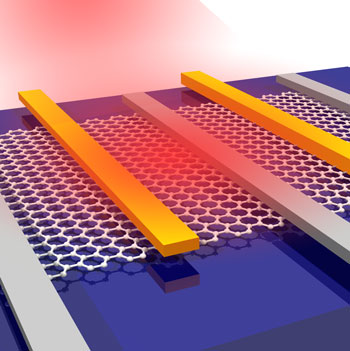 |
| Graphic representation of a metal-graphene-metal photodetectors with asymmetric metal contacts. (Source: IBM) |
| Xia explains that in previously fabricated graphene field-effect-transistor photodetectors the internal (built-in) electric fields, which are responsible for the separation of the photo-generated carriers, only exist in narrow regions (∼0.2 µm) adjacent to the electrode/graphene interfaces, where charge transfer between the metal and graphene leads to band bending. |
| "The absence of a strong electric field in the bulk graphene sheet, where most of the electron–hole pairs are generated, leads to carrier recombination without any contribution to the external photocurrent," he says. "In our work, we used multiple, interdigitated metal fingers, which leads to the creation of a greatly enlarged, high E-field, light-detection region. However, if both electrodes consist of the same metal, the built-in electric field profile in the channel between two neighboring fingers is symmetric, and the total photocurrent is zero." |
| The researchers therefore developed an asymmetric metallization scheme that can be used to break the mirror symmetry of the built-in potential profile within the channel, allowing for the individual contributions to be summed to give the overall photocurrent. |
| The IBM team says that the unique band structure of graphene can enable an ultrawide range of operational wavelengths, at least from 300 nm to 6 µm. Xia says that, in combination with its intrinsically high operating speed, this enables the graphene photodetector to be a promising candidate for a variety of applications including optical communications, remote sensing, environmental monitoring, terahertz detection, and surveillance. |
| The major challenge for wide-ranging applications of this technology is the production of large-scale and high quality graphene sheet. "Actually this is one of the major focuses of both graphene electronics and photonics research" says Xia. "If this can be realized, graphene can be used in a variety of photonic applications." |
 By
Michael
Berger
– Michael is author of four books by the Royal Society of Chemistry:
Nano-Society: Pushing the Boundaries of Technology (2009),
Nanotechnology: The Future is Tiny (2016),
Nanoengineering: The Skills and Tools Making Technology Invisible (2019), and
Waste not! How Nanotechnologies Can Increase Efficiencies Throughout Society (2025)
Copyright ©
Nanowerk LLC
By
Michael
Berger
– Michael is author of four books by the Royal Society of Chemistry:
Nano-Society: Pushing the Boundaries of Technology (2009),
Nanotechnology: The Future is Tiny (2016),
Nanoengineering: The Skills and Tools Making Technology Invisible (2019), and
Waste not! How Nanotechnologies Can Increase Efficiencies Throughout Society (2025)
Copyright ©
Nanowerk LLC
|

Become a Spotlight guest author! Join our large and growing group of guest contributors. Have you just published a scientific paper or have other exciting developments to share with the nanotechnology community? Here is how to publish on nanowerk.com. |
