| Posted: May 06, 2013 |
Improving AFM probe performance with a coat of graphene |
| (Nanowerk Spotlight) Most of the research efforts on developing synthesis methods for graphene has focused on flat substrates. Some groups have reported the formation of free-standing 3D graphene-based macroscopic structures (see for instance "Making graphene 'bread' – leavening technique results in freestanding graphene oxide films"). However, direct growth of graphene layers on prepatterned substrates has remained elusive. |
| In previous work, researchers led by James K. Gimzewski at UCLA have already shown that graphene grows continuously over large areas on different copper terraces without the underlying substrate morphology affecting the atomic arrangement of the grown material ("Continuity of Graphene on Polycrystalline Copper"). In new work, just reported in ACS Nano ("Graphene MEMS: AFM Probe Performance Improvement"), the team has applied this technique to grow graphene in prepatterned copper-coated substrates, and they apply this protocol for the fabrication of MEMS devices, in particular, atomic force microscope (AFM) probes. |
| "Conformal deposition of graphene on prepatterned substrates opens a multitude of device fabrication possibilities," writes Gimzewski. "One of them is the addition of different layers to the graphene, mostly by deposition, using the prepatterned substrate as a mold. This can result in hybrid 3D structures covered with graphene." |
| In this new work, the team demonstrates the fabrication of polymeric AFM probes covered by monolayer graphene that had been previously deposited on a prepatterned substrate. Furthermore, they show how graphene improves the functionality of the probes by making them conductive and more resistant to wear. |
| The fabrication steps utilized in the process are very standard and highly compatible with current silicon fabrication technology, which allows its application in any clean room or microtechnology laboratory. The entire process is based on the multiple spincoating, exposure, and development of SU-8 photoresist on a prestructured mold. |
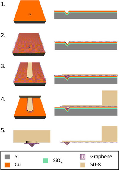 |
| Fabrication process scheme. Step 1 consists of preparing the silicon wafer by selectively etching the tip with KOH, growing a thermal silicon oxide, and finally coating the surface with copper. Step 2 is the CVD growth of a continuous layer of graphene due to the copper coating. During step 3, a thin layer of SU-8 is spin-coated, exposed, and developed in order to fill the tip mold and define the cantilever. Step 4 comprises an argon dry etch to remove the graphene elsewhere that is not already protected by SU-8. Also, a second and thicker layer of SU-8 is processed in order to shape the body of the probe. Finally, during step 5, the AFM probe is released without damaging the graphene layer by etching the silicon oxide with HF, the silicon with KOH, and the Cu with a commercially available Cu etchant solution. Probes are rinsed three times in DI water. (Reprinted with permission from American Chemical Society) |
| During this process, the copper layer is used as a seed layer for graphene growth (following the team's previously developed processing technique). |
| "The high temperatures of such a process might cause copper to sublime and even form islands on the patterned substrate if the layer is too thin," the researchers point out. "Thus, the copper layer thickness is chosen to ensure a continuous layer of graphene. We expect that annealing at higher pressures and optimizing growth conditions will allow decreasing the amount of copper deposited, which will lead to better AFM tip geometries." |
| To evaluate the properties of their graphene-coated AFM probes, the team compared them side by side with uncoated SU-8 probes that are fabricated with exact the same process except the CVD deposition of graphene. Using a commercial scanning probe microscope (SPM), they performed tapping mode and contact mode imaging. |
| "In our work, the tips' lifetime with the graphene layer is substantially improved, but comparison to any commercially available contact mode AFM probes is not fair at the moment, given our tips large original radius," says Gimzewski. |
| The team also tested the conductivity of the graphene layer on the AMP probe. The results show a conductive behavior, proving the continuity of the graphene layer on the AFM probe. |
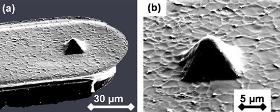 |
| Fabricated graphene-coated SU-8 AFM probes. SEM Micrographs: (a) released SU-8 AFM probe coated with graphene (background has been colored for improved contrast). (b) Zoom in of the tip showing again the continuity of the graphene and the dullness. (Reprinted with permission from American Chemical Society) |
| "Even though sharper tips need to be produced for these probes to be fully functional in any scanning experiment, they can be useful for some experiments as indentation on biological material," concludes Gimzewski. "In addition, this kind of device introduces the possibility of probing graphene properties by also using graphene. Until now, most of the experiments involving graphene are biased by the interactions of graphene with other materials. Graphene-coated AFM probes would allow studies on friction, adhesion, conductivity, etc. using graphene as a probing material and down at the nanoscale." |
 By
Michael
Berger
– Michael is author of four books by the Royal Society of Chemistry:
Nano-Society: Pushing the Boundaries of Technology (2009),
Nanotechnology: The Future is Tiny (2016),
Nanoengineering: The Skills and Tools Making Technology Invisible (2019), and
Waste not! How Nanotechnologies Can Increase Efficiencies Throughout Society (2025)
Copyright ©
Nanowerk LLC
By
Michael
Berger
– Michael is author of four books by the Royal Society of Chemistry:
Nano-Society: Pushing the Boundaries of Technology (2009),
Nanotechnology: The Future is Tiny (2016),
Nanoengineering: The Skills and Tools Making Technology Invisible (2019), and
Waste not! How Nanotechnologies Can Increase Efficiencies Throughout Society (2025)
Copyright ©
Nanowerk LLC
|

Become a Spotlight guest author! Join our large and growing group of guest contributors. Have you just published a scientific paper or have other exciting developments to share with the nanotechnology community? Here is how to publish on nanowerk.com. |
