Two-dimensional (2D) materials
Contents
Introduction to 2D Materials
Two-dimensional materials are part of a larger category of nanomaterials differentiated by their dimensions, specifically falling within the nanoscale range. These are materials that have a thickness of only a few atoms or even a single atom, giving them unique properties compared to their 3D counterparts.
A relatively new addition to the materials science domain, two-dimensional (2D) materials, also known as 2D nanomaterials, have shown great potential for revolutionizing various fields, from electronics to medicine.
The Importance of Dimensions in Nanomaterials
Nanomaterials are primarily categorized based on the dimensional characteristics they display. These dimensions are classified as zero-dimensional (0D), one-dimensional (1D), two-dimensional (2D), and three-dimensional (3D) nanomaterials, all of which fall within the nanoscale range.
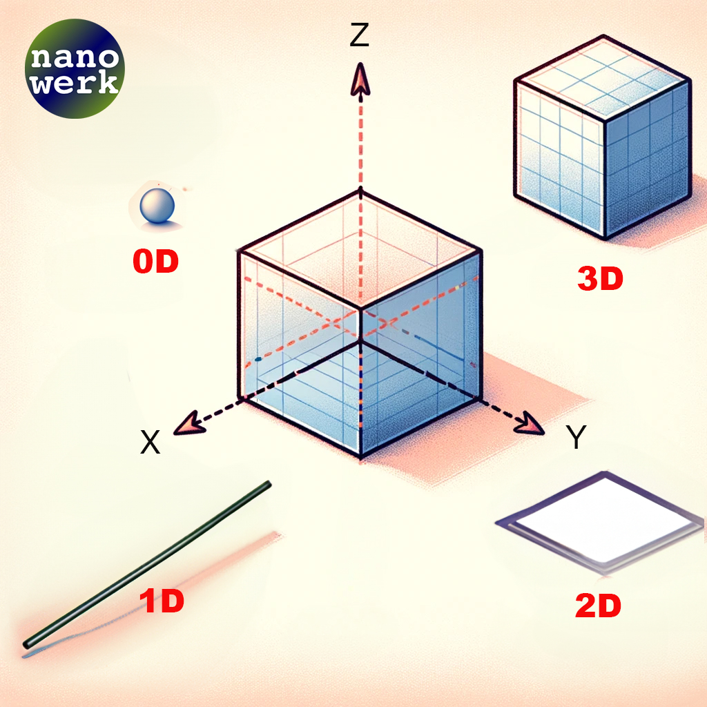
Classification of nanoscale dimensions. (© Nanowerk)
Quantum dots and small nanoparticles are often referred to as "zero-dimensional" (0D) structures, despite having three physical dimensions. This might sound confusing at first, but it’s because we’re talking about their quantum mechanical properties rather than their geometric shape. Let's unpack this a bit:
Quantum Confinement in All Three Dimensions: In quantum dots or small nanoparticles, electrons experience quantum confinement in all three dimensions, much like being restricted in an extremely tiny room. This confinement is effective when the size of the particle is comparable to or smaller than what is called the “exciton Bohr radius” of the material, which is typically a few nanometers This confinement limits the electrons to specific energy levels, their “discret energy levels.” Think of it as a game of musical chairs at the quantum scale: the electrons, like players in the game, can only occupy certain 'seats' or energy states.
The number of these available 'seats' is determined by several factors:
As a result of these combined factors, electrons in quantum dots have a limited set of energy levels they can occupy, akin to having a set number of chairs in the room. This is a stark contrast to larger, bulk materials where electrons have a more continuous range of energy levels available.
Exciton Bohr Radius: The exciton Bohr radius is a key factor in determining the size limit. It is like a measuring stick that tells us how small we need to make our nanoparticle to see its cool quantum effects. It varies between materials but is generally in the range of a few nanometers. When the size of the nanoparticle is smaller than or similar to this radius, quantum confinement effects are significant, and the particle behaves as a 0D system.
Size and Quantum Effects: The size of quantum dots is typically 2-10 nanometers. At this scale, the quirky rules of quantum mechanics start to dominate, making these particles behave very differently from larger pieces of the same material.
Comparison with Higher Dimensions: In our room analogy above, think of 1D and 2D materials, like nanowires and thin films, as narrow hallways and wide floors. Electrons can move freely along these hallways or floors but can’t jump out of them. This partial freedom leads to different behaviors compared to the completely confined quantum dots or nanoparticles.
Transition to 3D Behavior: As the size of the nanoparticle gets bigger, beyond the exciton Bohr radius, it starts behaving more like a regular, bulk material. The electrons begin to move more freely, akin to how water starts to flow when a dam is opened, leading to a more continuous range of energy levels. This marks the transition towards 3D behavior.
Material-Dependent Threshold: The exact size at which this transition occurs depends on the material of the nanoparticle. Different materials have different exciton Bohr radii and therefore different thresholds for the transition from quantum-confined (0D) behavior to bulk-like (3D) behavior.
Gradual Transition: It's important to note that the transition from 0D to 3D behavior is not abrupt but gradual. As the nanoparticle grows, its energy levels slowly spread out, moving from distinct steps on a ladder to more of a ramp. Accordingly, a material's physical properties change as the energy levels evolve from discrete to continuous.
To specifically address two-dimensional (2D) nanomaterials, they represent a unique class within the nanomaterials spectrum. In 2D systems, such as graphene and other ultra-thin films, electrons are confined in two dimensions, allowing movement only along the plane of the material. This confinement creates distinctive energy states, profoundly influencing the material's electrical, thermal, and mechanical properties. Unlike 0D structures where quantum confinement occurs in all three dimensions, 2D materials exhibit confinement in only two, leading to different quantum mechanical behaviors and applications. These materials are known for their exceptional strength, flexibility, and conductivity, making them crucial in advancing nanotechnology and electronics. As with 0D materials, the properties of 2D materials are heavily influenced by their size and shape, but they also exhibit phenomena unique to their two-dimensional nature, such as high surface area to volume ratios and novel electronic behaviors that are not seen in their bulk counterparts.
Exploring the Properties of 2D Materials
The special properties of 2D materials stem from their incredibly thin structure. 2D materials, with their high surface area to volume ratio, remarkable mechanical strength, and superior electronic conductivity, possess extraordinary physical and chemical properties that distinguish them from their 3D bulk counterparts. They have stirred immense interest in the scientific community, leading to innovative applications in various fields.
One of the significant advantages of 2D materials is their high surface area, making them perfect for catalytic reactions. Moreover, their exceptional electronic conductivity propels their use in electronics and energy storage devices. Due to their thin, flat structure, 2D materials can be layered or stacked in different combinations, known as van der Waals heterostructures, to create new materials with customized properties. This opens up a world of possibilities for new, ground-breaking applications.
Types of 2D Materials
The most famous 2D material, graphene, is stronger than steel, an excellent conductor of heat and electricity, and almost entirely transparent.
In recent years, there has been a surge in research into 2D layered materials and their hybrids, prompted by the unique optical and electronic properties of graphene, and its potential applications, particularly in nanoelectronics. MXenes and atomic layered crystals, including transition metal dichalcogenides (TMDs), semiconducting dichalcogenides, monoatomic buckled crystals like phosphorene, and diatomic hexagonal boron nitride, form part of this broad spectrum of 2D materials.
Manufacturing and Synthesis of 2D Materials
These materials can either be obtained by exfoliating bulk materials down to smaller scales or via epitaxial growth and chemical vapor deposition (CVD) for larger areas.
The manufacturing and synthesis of 2D materials is a critical aspect of their application in various fields. Given the thinness of these materials – often just one to a few atoms thick – their manufacturing processes differ significantly from those of traditional 3D materials. Here are the most prominent methods:
Mechanical Exfoliation
Mechanical exfoliation, also known as the "Scotch tape method," was the first method used to isolate graphene, the first 2D material ever discovered. This process involves using adhesive tape to peel off layers from a piece of graphite, resulting in thin flakes of graphene. While this method is simple and inexpensive, it doesn't lend itself to large-scale production and the size and quality of the graphene produced can be inconsistent.
Chemical Vapor Deposition (CVD)
Chemical vapor deposition is a widely used method for producing high-quality, large-area 2D materials. In this process, a substrate (typically a metal) is exposed to one or more volatile precursors, which react or decompose on the substrate surface to produce the desired material. For example, in the case of graphene, a common method is to expose a copper substrate to methane gas at high temperatures. The methane decomposes, and the carbon atoms arrange themselves into a graphene layer on the copper surface. This method can produce high-quality 2D materials but is complex and requires precise control of temperature and pressure.
Liquid-phase Exfoliation
Liquid-phase exfoliation involves dispersing layered materials into a liquid medium and then applying ultrasonic energy to separate the layers into individual, atomically thin flakes. This method has the potential for large-scale production of 2D materials and can produce materials with a range of layer numbers, sizes, and shapes. However, it may result in lower-quality materials than other methods, and the choice of liquid medium can significantly influence the results.
Molecular Beam Epitaxy (MBE)
Molecular Beam Epitaxy is a highly controlled deposition technique used to create single layers of atoms. This is accomplished by heating elemental sources, which then travel to the substrate where they condense and form the 2D material. This method allows for high precision and control over the structure of the 2D material.
Each of these methods has its own advantages and challenges, and the choice of method depends on factors such as the specific 2D material being produced, the desired properties of the material, and the intended application. As research progresses, these methods are being continually improved, and new methods are being developed to more efficiently and effectively produce high-quality 2D materials.
Applications of 2D Materials
2D materials, with their unique properties and characteristics, are finding a variety of uses across different industries. Here are a few key areas where these materials have begun to show significant potential:
Electronics
The semiconductor industry has been one of the first to explore the potential of 2D materials. Graphene, for example, has been extensively studied for its exceptional electronic properties. It exhibits high electron mobility, making it a potent material for future high-speed electronic devices, including transistors and sensors. Moreover, other 2D materials, such as molybdenum disulfide (MoS2), are being investigated for their semiconducting properties, offering a possible alternative to silicon in future electronics.
Energy Storage and Conversion
2D materials also offer great promise in the field of energy storage and conversion. With their high surface area and exceptional electrical properties, they can greatly enhance the performance of batteries and supercapacitors. They can also play a critical role in solar cells and fuel cells. For instance, graphene can improve the efficiency of solar cells, while transition metal dichalcogenides can be used as effective catalysts in hydrogen production.
Biomedical Applications
The biomedical field is another area where 2D materials are expected to make a substantial impact. Given their biocompatibility and functionalization potential, these materials can be used in drug delivery systems, biosensing, bioimaging, and tissue engineering. For example, graphene and its derivatives have been explored for drug delivery applications due to their ability to readily conjugate with various biomolecules.
Sensors and Detectors
2D materials, due to their high surface-to-volume ratio and excellent electrical properties, can be used to develop highly sensitive and fast-responding sensors. For example, graphene-based sensors have been shown to detect individual gas molecules, paving the way for highly accurate air quality monitoring systems. Similarly, molybdenum disulfide has been used to create flexible photodetectors with high light sensitivity.
The Future of 2D Materials
Two-dimensional (2D) materials, since their debut with graphene, have been the subject of intense research. Their ultra-thin structure combined with unique and often extraordinary properties positions them at the forefront of several scientific and technological revolutions.
Emerging 2D Materials
While graphene, transition metal dichalcogenides (TMDCs), black phosphorus, and hexagonal boron nitride (h-BN) are well-known 2D materials, new ones are constantly being discovered and synthesized. Examples include phosphorene, stanene, and germanene, each possessing unique properties that lend themselves to various applications.
Phosphorene, a monolayer of black phosphorus, exhibits a direct bandgap and high carrier mobility, making it suitable for optoelectronics and nanoelectronics. Stanene and germanene, on the other hand, are predicted to be topological insulators, materials that conduct electricity on the surface but act as insulators in the bulk. This could potentially revolutionize quantum computing and spintronics.
Advancements in Manufacturing Techniques
The scalability of 2D material production is a critical factor in their practical application. While methods such as mechanical exfoliation and chemical vapor deposition have been employed successfully, there are ongoing efforts to improve and discover new production methods. For instance, roll-to-roll production, a technique borrowed from the paper industry, is being adapted for the mass production of 2D materials, promising a future where these materials become commonplace.
Application Areas on the Horizon
The potential applications for 2D materials continue to expand as our understanding grows. For example, in the realm of quantum technology, 2D materials could serve as the building blocks for quantum bits, or qubits, the fundamental units of quantum computers.
In the field of energy, the high surface area of 2D materials could enhance the performance of batteries and supercapacitors. Plus, the photovoltaic effect seen in some 2D materials could be harnessed for more efficient solar cells.
Biomedicine is another sector that could benefit tremendously from these materials. From drug delivery to biosensing and tissue engineering, the possibilities are virtually endless.
Challenges and Opportunities
While the future of 2D materials is promising, it is not without challenges. Issues with stability, production scalability, and integration into existing technologies must be addressed. However, these challenges also present opportunities for innovation and discovery. As researchers and engineers worldwide continue to explore the potential of 2D materials, the coming years will undoubtedly bring exciting developments.
In conclusion, the journey into the world of 2D materials is just beginning. Their unique properties and vast potential signal a new era in materials science, capable of shaping the future of numerous industries. As we dive deeper into the exploration of these extraordinary materials, their transformative power is anticipated to unfold, making the world of 2D materials a truly exciting frontier.
As we deepen our understanding of 2D materials and continue to refine our abilities to manipulate and manufacture them, we can expect the range of their applications to broaden. This is an exciting field of study, and we're just beginning to scratch the surface of the possibilities these materials hold.
If you want to delve deeper into this topic, we recommend reading this review article in iScience "Prospective applications of two-dimensional materials beyond laboratory frontiers: A review".
Frequently Asked Questions (FAQs) about 2D Materials
What are 2D materials?
2D materials, also known as two-dimensional materials, are substances composed of a single layer of atoms. They are considered 2D because they extend in only two dimensions: length and width. The most popular example of a 2D material is graphene, a single layer of carbon atoms arranged in a hexagonal lattice.
Why are 2D materials important?
2D materials are important because of their unique properties that aren't found in their 3D counterparts. These properties include exceptional strength, flexibility, transparency, and high electron mobility. As such, 2D materials hold great potential for applications in various fields like electronics, sensors, energy storage, and quantum computing.
What are the different types of 2D materials?
There are several types of 2D materials including graphene, transition metal dichalcogenides (TMDs) like molybdenum disulfide (MoS2), hexagonal boron nitride (hBN), and phosphorene. Each 2D material has unique properties that make them suitable for different applications.
How are 2D materials made?
2D materials are typically made using various top-down and bottom-up fabrication techniques. The most well-known method is mechanical exfoliation, also known as the "scotch tape method", which was used to isolate graphene. Other techniques include chemical vapor deposition (CVD), liquid exfoliation, and epitaxial growth.
What is the potential application of 2D materials in electronics?
2D materials are promising for electronics due to their high electron mobility, flexibility, and the possibility for miniaturization. They could be used in the development of ultra-thin and flexible electronic devices, including transistors, sensors, and photodetectors. Their high thermal conductivity also makes them suitable for thermal management applications in electronics.
How do 2D materials contribute to energy storage?
2D materials can greatly enhance the performance of energy storage devices. For instance, they can be used in supercapacitors due to their large surface area, and in batteries as electrode materials to increase energy density. They can also be incorporated in fuel cells to increase their efficiency.
What are the challenges in using 2D materials?
While 2D materials hold great potential, there are also challenges in their use. These include difficulty in producing high-quality 2D materials at a large scale, control of their properties, and integration into existing technology. In addition, more research is needed to fully understand their properties and potential impact on the environment and health.
How do 2D materials compare to traditional materials?
Compared to traditional 3D materials, 2D materials exhibit unique properties such as higher strength, transparency, and better charge mobility. However, 2D materials are generally more difficult to manufacture and handle due to their ultra-thin nature. They also require more research to understand their potential implications fully.
What is the environmental impact of 2D materials?
The environmental impact of 2D materials is still being researched. While they could potentially lead to more energy-efficient technologies, concerns exist about their manufacturing process and disposal. It's essential to develop environmentally friendly methods for 2D material production and disposal to mitigate any potential negative impact.
What is the future of 2D materials?
The future of 2D materials is promising, with extensive ongoing research exploring their potential applications. As our understanding and ability to manufacture these materials improves, we can expect to see 2D materials being increasingly used in various technology areas like electronics, energy, sensors, and even quantum computing.
 By
Michael
Berger
– Michael is author of four books by the Royal Society of Chemistry:
Nano-Society: Pushing the Boundaries of Technology (2009),
Nanotechnology: The Future is Tiny (2016),
Nanoengineering: The Skills and Tools Making Technology Invisible (2019), and
Waste not! How Nanotechnologies Can Increase Efficiencies Throughout Society (2025)
Copyright ©
Nanowerk LLC
By
Michael
Berger
– Michael is author of four books by the Royal Society of Chemistry:
Nano-Society: Pushing the Boundaries of Technology (2009),
Nanotechnology: The Future is Tiny (2016),
Nanoengineering: The Skills and Tools Making Technology Invisible (2019), and
Waste not! How Nanotechnologies Can Increase Efficiencies Throughout Society (2025)
Copyright ©
Nanowerk LLC
