Chemical vapor deposition (CVD) and its role in semiconductor fabrication
Contents
Chemical Vapor Deposition (CVD) is a widely used technique in materials science, particularly in the fabrication of thin films and coatings, as well as the synthesis of advanced materials. It involves the deposition of materials onto a substrate through the chemical reaction of gaseous precursors. CVD processes have been instrumental in the development of semiconductor devices, nanomaterials, and various protective coatings.
Chemical vapor deposition also is a promising approach for scalable synthesis of 2D materials – but automated commercial systems can be cost prohibitive for some research groups and startup companies. To address this, resarchers have released the open-source design of a chemical vapor deposition (CVD) system for two-dimensional (2D) materials growth.
One key application of CVD is in the manufacturing of Complementary Metal-Oxide-Semiconductor (CMOS) technology, which is widely used in integrated circuits, microprocessors, and memory chips.
CVD Process Steps in CMOS Fabrication
The CVD process can be broken down into the following steps:
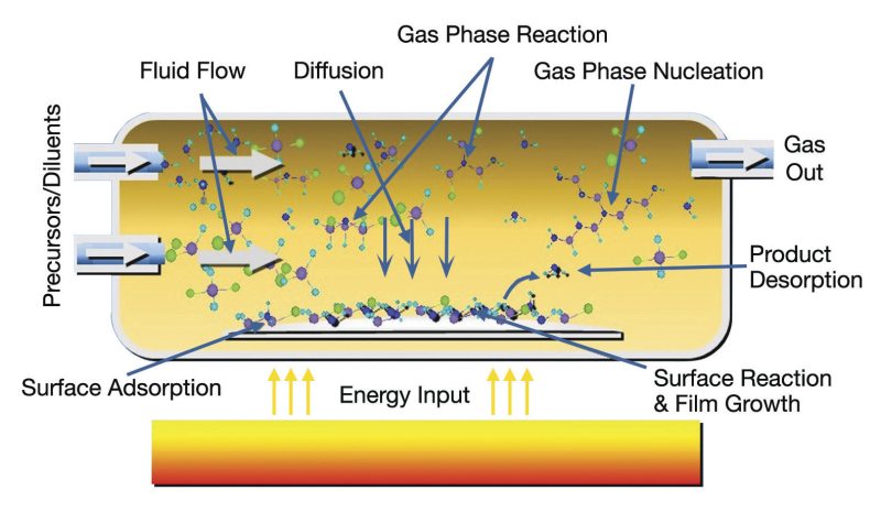
1. Introduction of reactants: Gaseous precursors are introduced into a reaction chamber containing the substrate. These precursors are typically delivered through a carrier gas or directly as a gas/vapor. The selection of precursors depends on the desired material and deposition conditions. In many cases, precursor delivery systems are designed to ensure precise control over the precursor flow rate, enabling the regulation of the concentration within the reaction chamber. Common precursors for CMOS technology involve metal-organic compounds, hydrides, and halides. The choice of carrier gas, which is usually an inert gas such as nitrogen or argon, is also essential, as it can influence the transport of precursor molecules and the overall deposition process.
2. Activation of reactants: The precursors require activation to initiate the chemical reaction, which can be achieved through various methods. In thermal CVD, the temperature of the reaction chamber or the substrate is raised to facilitate the reaction. Plasma-enhanced CVD (PECVD) involves the generation of a plasma to provide the energy necessary for precursor activation. In catalytic CVD, a catalyst is introduced to lower the energy barrier for the reaction to occur. The activation method is chosen based on the specific requirements of the deposition process, such as the desired deposition rate, film properties, and substrate compatibility. The activation step is crucial in determining the reaction kinetics and the overall efficiency of the CVD process.
3. Surface reaction and deposition: Activated precursors react at the substrate surface, forming the desired material. The reaction products are then deposited onto the substrate as a thin film. The surface reactions may involve several surface-mediated processes, such as adsorption of precursor molecules onto the substrate, surface diffusion of adsorbed species, chemical reactions between adsorbed species or with the substrate, and desorption of byproducts. These reactions can be influenced by the substrate temperature, precursor concentration, and pressure within the reaction chamber. The deposition rate, film thickness, and film properties are controlled by optimizing these factors to ensure the desired outcome in terms of film quality and uniformity.
4. Removal of byproducts: The byproducts of the chemical reaction, which can be volatile or non-volatile, must be eliminated from the reaction chamber. Volatile byproducts are typically carried away by the gas flow, while non-volatile byproducts may necessitate additional cleaning steps or in situ removal techniques. Efficient removal of byproducts is essential to prevent contamination of the deposited film and maintain a clean environment within the reaction chamber. Proper byproduct management also helps reduce the risk of particle formation, which can lead to defects in the film and adversely affect the performance of CMOS devices. In some cases, byproduct removal may require sophisticated gas handling systems, including scrubbers or abatement systems, to minimize environmental impact and ensure compliance with safety regulations.
CVD Processes Classification in CMOS Technology
CVD processes can be broadly classified into several categories based on the type of energy source used for activation:
Thermal CVD
In thermal CVD, the reaction is driven by the thermal energy supplied by heating the substrate or the reaction chamber. Precursor molecules are activated when they come into contact with the heated substrate or when they absorb energy from the heated environment. This is the most common form of CVD for CMOS technology and can be further divided into: a. Low-pressure CVD (LPCVD): This process operates at reduced pressures (typically below atmospheric pressure), which allows for better control over the gas flow, improved uniformity, and reduced gas-phase reactions.
LPCVD is often used for depositing high-quality, conformal films in CMOS fabrication. b. Atmospheric pressure CVD (APCVD): This process operates at atmospheric pressure and is generally simpler and more cost-effective than LPCVD. However, it may have lower film quality and uniformity compared to LPCVD.
Plasma-enhanced CVD (PECVD)
In PECVD, a plasma is used to provide the energy needed for the chemical reaction. The plasma is generated by applying an electric field to the reaction chamber, which ionizes the precursor gas molecules and creates a highly reactive environment.
PECVD can be performed at lower temperatures compared to thermal CVD, making it suitable for heat-sensitive substrates in CMOS fabrication. Additionally, PECVD can enhance the deposition rate and modify the film properties by controlling the plasma parameters.
Photochemical CVD
In this process, the energy required for the chemical reaction is provided by ultraviolet (UV) or visible light. The light source (usually a high-intensity lamp or laser) excites the precursor molecules, leading to the formation of reactive species that can then react on the substrate surface to form the desired film.
Photochemical CVD allows for lower temperature deposition and better control of film properties in CMOS technology. This technique is particularly useful for depositing materials with unique properties, such as those with a high degree of crystallinity or specific optical characteristics.
Metal-organic CVD (MOCVD)
This method uses metal-organic compounds as precursors, which typically contain a metal center bonded to one or more organic ligands. These precursors are introduced into the reaction chamber, where they are thermally decomposed or activated by other means, such as plasma or light. The metal center reacts with other precursor molecules or the substrate to form the desired material, while the organic ligands are released as byproducts.
MOCVD is particularly useful for the deposition of compound semiconductors, high-quality dielectric films, and metal films in CMOS devices. It also allows for the precise control of composition and doping levels in the deposited films.
Atomic Layer Deposition (ALD)
Atomic Layer Deposition is a special type of CVD that involves sequential, self-limiting surface eactions, resulting in atomic-level control of film thickness and excellent conformality. The ALD process alternates between the introduction of two or more precursor gases into the reaction chamber. Each precursor reacts with the substrate or the previously deposited layer, forming a chemisorbed monolayer. Once the surface is fully saturated with the chemisorbed species, the excess precursor and reaction byproducts are purged from the chamber before introducing the next precursor. This cycle is repeated until the desired film thickness is achieved.
ALD is critical for the fabrication of advanced CMOS devices with increasingly smaller feature sizes and higher performance requirements, as it provides precise control over film thickness, composition, and doping levels.
Advantages and Challenges of CVD in CMOS Technology
The CVD process offers numerous advantages over other deposition techniques, making it the method of choice for CMOS technology. Some of these advantages include:
Excellent uniformity
CVD enables the deposition of highly uniform thin films, which is crucial for the performance and reliability of CMOS devices. Uniform films ensure consistent electrical, optical, and mechanical properties across the entire surface of the device, minimizing performance variations and improving device yield. Uniformity is particularly important for large-area substrates and advanced devices with complex architectures, where variations in film thickness or composition can lead to device failure or reduced functionality. The uniformity provided by CVD is achieved through precise control of process parameters such as temperature, pressure, and precursor concentration, as well as the conformal nature of the deposition process.
Conformality
CVD is capable of depositing materials on complex surfaces with high aspect ratios, ensuring that all critical features of CMOS devices are coated evenly. This is essential for advanced devices with three-dimensional structures, such as FinFETs or 3D NAND memory cells, where conformal coverage is necessary to achieve the desired device performance and reliability.
Conformal films also improve the electrical isolation between adjacent features, reducing the risk of short circuits or leakage currents. The conformality of CVD processes is mainly due to the surface-mediated nature of the reactions, allowing for the deposition of materials on both horizontal and vertical surfaces.
Scalability
CVD is a highly scalable process, allowing for the production of CMOS devices on large substrates or even at the wafer scale, which is essential for cost-effective manufacturing. The scalability of CVD processes enables the transition from laboratory-scale research to high-volume production, making it an attractive technique for the semiconductor industry.
Furthermore, the ability to process multiple wafers simultaneously in a single reaction chamber can significantly increase production throughput and reduce manufacturing costs. The scalability of CVD also facilitates the integration of multiple process steps, such as deposition and annealing, within the same reaction chamber, further enhancing production efficiency.
Material versatility
CVD can be used to deposit a wide range of materials, including metals, dielectrics, and semiconductors, providing flexibility in the design and fabrication of CMOS devices. This versatility allows for the exploration of novel materials and device architectures, leading to improvements in device performance, energy efficiency, and reliability. The ability to deposit different materials using the same CVD equipment can also simplify the manufacturing process and reduce the capital investment required for device fabrication.
The versatility of CVD processes is a result of the wide range of precursor chemistries and process conditions that can be used to tailor the deposition of specific materials and achieve the desired film properties.
These advantages make CVD a preferred method for CMOS technology, as they directly contribute to improved device performance, reliability, and cost-effectiveness. By leveraging the strengths of CVD processes, semiconductor manufacturers can continue to push the boundaries of CMOS device scaling and performance, meeting the increasing demands for more powerful and efficient electronic devices.
However, CVD also presents some challenges, including:
Handling of toxic and/or reactive precursor gases
Some precursors used in CVD processes can be hazardous, posing risks to both human health and the environment. These precursors may be toxic, flammable, or reactive, requiring special handling, storage, and disposal practices to minimize exposure and ensure safety. Implementing appropriate safety measures, such as gas cabinets, gas monitoring systems, and abatement equipment, can increase the complexity and cost of the CVD process. Additionally, the use of hazardous precursors may be subject to strict regulations and compliance requirements, further increasing the operational burden for manufacturers.
Potential contamination from residual byproducts
The presence of byproducts in the reaction chamber can lead to contamination of the deposited films, impacting the performance of CMOS devices. Contaminants can introduce defects, such as pinholes or particulates, which can compromise device functionality or lead to premature failure. Thus, maintaining a clean environment and implementing effective byproduct removal strategies are crucial. This may involve the use of purifiers, filters, and advanced cleaning techniques to minimize contamination risks. Furthermore, the need for strict contamination control can make the CVD process more complex and potentially increase manufacturing costs.
Precise control of process parameters
CVD processes require accurate control of various parameters, such as temperature, pressure, and precursor concentration, to ensure the desired film properties and thickness. Precise control can be challenging, particularly when scaling up the process for large-scale production. Maintaining uniform temperature and pressure profiles across large substrates or multiple wafers can require sophisticated equipment and advanced process control strategies.
Additionally, the optimization of process parameters may be time-consuming and require extensive experimentation, particularly when developing new materials or device architectures.
Equipment and operational costs
The complexity of CVD processes and the need for precise control can lead to high equipment and operational costs. CVD reactors, gas handling systems, and associated monitoring and control equipment can represent significant capital investments for manufacturers. Furthermore, the ongoing costs associated with precursor consumption, waste disposal, and maintenance can add to the overall cost of the CVD process. These costs can be particularly challenging for smaller manufacturers or those working with novel materials or processes, where economies of scale may not yet be realized.
Comparing Physical Vapor Deposition and Chemical Vapor Deposition
While both Physical Vapor Deposition (PVD) and CVD are used for creating thin films and coatings, their methodologies, applications, and the properties of the resulting films can vary significantly. Understanding these differences is crucial for selecting the appropriate technology for specific applications.
Methodology
- PVD: Involves the physical transition of a material from a condensed phase to a vapor phase by sputtering or evaporation in a vacuum environment, followed by deposition on the substrate. The process is primarily physical, and the deposited materials are generally the same as the source materials.
- CVD: Relies on chemical reactions between gaseous precursors and the substrate to deposit materials in the form of a thin film. These reactions occur at relatively high temperatures, and the deposited material is often different from the gaseous precursors due to the chemical reactions involved.
Material Properties
- PVD Coatings: Tend to be thinner and have a high purity level, with excellent adhesion and uniformity. PVD allows for the deposition of a wide range of materials, including metals, alloys, and ceramics, with precise control over the film's structure and properties.
- CVD Coatings: Can be deposited at a thicker rate compared to PVD and are excellent for conformal coatings over complex geometries. CVD films can also exhibit high purity and excellent adhesion but are particularly noted for their ability to fill gaps and provide uniform coatings on intricate surfaces.
Applications
- PVD: Widely used in the electronics industry for semiconductor devices, decorative coatings for wear resistance (e.g., watches, automotive), and tools for enhanced durability.
- CVD: Commonly used for semiconductor manufacturing, where uniform coatings are essential, and in the creation of wear-resistant coatings, optical films, and various types of sensors.
Advantages and Limitations
- PVD: Offers a cleaner process with less environmental impact compared to CVD, as it typically does not involve toxic or hazardous chemicals. However, it may not be as effective for coating complex or porous surfaces.
- CVD: Can produce higher quality films with better step coverage and conformity around complex shapes. However, it often requires higher temperatures and involves the use of hazardous chemicals, raising environmental and safety concerns.
To sum it all up, both PVD and CVD have their unique strengths and weaknesses, making them suitable for different applications. The choice between PVD and CVD will depend on the specific requirements of the coating, including the desired material properties, the complexity of the substrate's shape, environmental considerations, and cost constraints.
Conclusion
Despite these challenges, the advantages offered by CVD processes often outweigh the drawbacks, making CVD a critical technology in the fabrication of advanced materials and devices, including CMOS technology. By addressing these challenges through ongoing research and development, improvements in process control, and the adoption of innovative techniques and materials, the role of CVD in CMOS fabrication is expected to continue growing, enabling the development of smaller, more powerful, and more efficient electronic devices.
