Exploring Physical Vapor Deposition: A Pathway to Advanced Coating Technologies
Definition: Physical Vapor Deposition (PVD) is a sophisticated coating technology widely used to deposit thin films of materials onto various substrates. This technique involves the physical transition of a material from a condensed phase, which can be either solid or liquid, into a vapor phase and then back to a condensed phase in the form of a thin film, through processes such as sputtering, evaporation, or ion plating. PVD enables the production of high-purity, high-performance, and durable coatings that enhance the properties of the substrate material, such as its resistance to wear, corrosion, and oxidation.
Fundamental Principles and Methodologies
PVD coating processes are primarily vacuum-based techniques that ensure the deposition of thin films in a controlled environment. The process begins with the generation of a material vapor through physical means, such as heating (thermal evaporation) or bombardment with ions (sputtering). The vaporized atoms then travel through a vacuum to the substrate, where they condense to form a thin film. The specific properties of the deposited film, including its thickness, composition, and crystal structure, can be precisely controlled through parameters such as temperature, deposition rate, and the nature of the substrate.
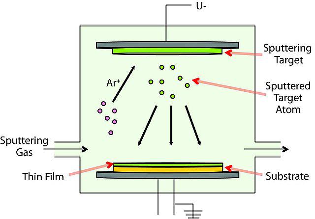
How Physical Vapor Deposition Works
The choice of PVD technique depends on the material to be deposited, the desired film properties, and the specific application requirements. Thermal evaporation, one of the simplest forms of PVD, involves heating a material in a vacuum until it vaporizes. In contrast, sputtering uses ions generated in a plasma to knock atoms from the target material, which then deposit on the substrate. Ion plating combines physical sputtering with chemical reactions to enhance film adhesion and density.
Key Features of Physical Vapor Deposition
PVD coatings are known for several distinct advantages:
- High Purity and Uniformity: Films produced by PVD are of high purity and have uniform thickness, which is essential for many industrial and research applications.
- Excellent Adhesion: The physical bonding process ensures excellent adhesion of the film to the substrate.
- Diverse Material Compatibility: PVD can deposit a wide range of materials, including metals, alloys, and ceramics, on various substrates.
- Enhanced Durability: Coatings are highly durable, offering improved wear, corrosion, and oxidation resistance.
Limitations of Physical Vapor Deposition
While PVD offers numerous benefits, it also has limitations:
- Equipment Cost: The initial investment for PVD equipment can be high, making it less accessible for small-scale operations.
- Process Complexity: Achieving uniform coatings on complex geometries can be challenging and may require specialized fixtures or multiple processing steps.
Applications of Physical Vapor Deposition
PVD technologies have found applications across a broad spectrum of industries:
- Microelectronics: PVD is crucial for depositing thin films of metals and dielectrics in the fabrication of integrated circuits and semiconductor devices. It enables the creation of conductive pathways, barriers, and insulating layers with precise control over composition and thickness.
- Decorative Coatings: The technique is used to deposit metallic and alloy coatings on consumer products such as watches, jewelry, and automotive parts to enhance their appearance and resistance to tarnishing and wear.
- Protective Coatings: Tools and machine parts are coated with hard, wear-resistant materials like titanium nitride to extend their service life and performance in demanding environments.
- Optical Applications: PVD is employed to produce reflective and anti-reflective coatings for optical components, improving the efficiency and durability of lenses, mirrors, and displays.
- Solar Panels: Thin-film photovoltaic cells rely on PVD for the deposition of materials that convert sunlight into electricity, offering a cost-effective alternative to traditional silicon-based solar cells.
- Medical Devices: Biocompatible coatings applied via PVD enhance the performance and longevity of medical implants and instruments.
Comparing Physical Vapor Deposition and Chemical Vapor Deposition
While both PVD and Chemical Vapor Deposition (CVD) are used for creating thin films and coatings, their methodologies, applications, and the properties of the resulting films can vary significantly. Understanding these differences is crucial for selecting the appropriate technology for specific applications.
Methodology
- PVD: Involves the physical transition of a material from a condensed phase to a vapor phase by sputtering or evaporation in a vacuum environment, followed by deposition on the substrate. The process is primarily physical, and the deposited materials are generally the same as the source materials.
- CVD: Relies on chemical reactions between gaseous precursors and the substrate to deposit materials in the form of a thin film. These reactions occur at relatively high temperatures, and the deposited material is often different from the gaseous precursors due to the chemical reactions involved.
Material Properties
- PVD Coatings: Tend to be thinner and have a high purity level, with excellent adhesion and uniformity. PVD allows for the deposition of a wide range of materials, including metals, alloys, and ceramics, with precise control over the film's structure and properties.
- CVD Coatings: Can be deposited at a thicker rate compared to PVD and are excellent for conformal coatings over complex geometries. CVD films can also exhibit high purity and excellent adhesion but are particularly noted for their ability to fill gaps and provide uniform coatings on intricate surfaces.
Applications
- PVD: Widely used in the electronics industry for semiconductor devices, decorative coatings for wear resistance (e.g., watches, automotive), and tools for enhanced durability.
- CVD: Commonly used for semiconductor manufacturing, where uniform coatings are essential, and in the creation of wear-resistant coatings, optical films, and various types of sensors.
Advantages and Limitations
- PVD: Offers a cleaner process with less environmental impact compared to CVD, as it typically does not involve toxic or hazardous chemicals. However, it may not be as effective for coating complex or porous surfaces.
- CVD: Can produce higher quality films with better step coverage and conformity around complex shapes. However, it often requires higher temperatures and involves the use of hazardous chemicals, raising environmental and safety concerns.
To sum it all up, both PVD and CVD have their unique strengths and weaknesses, making them suitable for different applications. The choice between PVD and CVD will depend on the specific requirements of the coating, including the desired material properties, the complexity of the substrate's shape, environmental considerations, and cost constraints.
The Future of Physical Vapor Deposition
As advancements in PVD technology continue, the potential applications are expanding. Innovations in process control, equipment design, and material science are expected to open new frontiers in nanotechnology, energy storage, and beyond, further solidifying PVD's role in the next generation of coating technologies.
