CMOS Technology Explained
Content
Complementary Metal-Oxide-Semiconductor (CMOS) technology is a vital part of modern electronics, used in designing and manufacturing integrated circuits (ICs) that power many digital devices. CMOS technology combines two types of transistors that work together, leading to efficient power use and high noise immunity.
The Building Blocks – nMOS and pMOS Transistors
CMOS technology uses two different types of transistors, n-type (nMOS) and p-type (pMOS), which work together in pairs in a complementary manner. The term "complementary" refers to how these two transistor types interact with each other to create a more efficient and reliable circuit. By working together, nMOS and pMOS transistors enable CMOS circuits to consume less power and be more resistant to electronic noise.
In a CMOS circuit, the nMOS and pMOS transistors are arranged in a way that, when one transistor is conducting (switched on), the other is non-conducting (switched off). This complementary configuration prevents any significant current from flowing through the circuit when it is in a stable state (either high or low). The result is low power consumption because very little energy is wasted as heat.
For example, consider a simple CMOS inverter circuit. An inverter takes an input signal and produces an output signal that is the opposite or the inverse of the input. In this circuit, the nMOS transistor is connected to the ground, while the pMOS transistor is connected to the power supply. When the input signal is high (logic 1), the nMOS transistor turns on, and the pMOS transistor turns off. The output is then connected to the ground through the nMOS transistor, resulting in a low (logic 0) output. Conversely, when the input signal is low (logic 0), the pMOS transistor turns on, and the nMOS transistor turns off. The output is then connected to the power supply through the pMOS transistor, resulting in a high (logic 1) output. In both cases, only one of the transistors is conducting, minimizing power consumption.
The complementary nature of nMOS and pMOS transistors also contributes to CMOS circuits' high noise immunity. Noise immunity refers to a circuit's ability to function correctly even in the presence of electrical interference or noise. Since the nMOS and pMOS transistors work together, they create a wide voltage margin between the high and low logic levels, making it more difficult for noise to cause a false signal or error in the circuit.
In summary, the complementary arrangement of nMOS and pMOS transistors in CMOS technology allows for efficient power utilization and high noise immunity. This unique configuration makes CMOS circuits ideal for a wide range of electronic devices that require energy efficiency and reliable operation.
Here's a simple explanation of the differences between these two transistor types:
nMOS Transistors:
pMOS Transistors;
The CMOS Fabrication Process: Transforming Silicon Wafers into Integrated Circuits
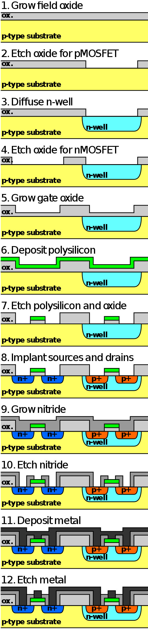
The fabrication of CMOS transistors is a highly intricate process that involves several steps, each of which plays a crucial role in ensuring the functionality and reliability of the final product. Here, we delve deeper into the main stages of CMOS transistor fabrication:
Formation of an insulating layer on a silicon wafer
The process begins with a silicon wafer, which serves as the substrate for the transistors. To prevent electrical shorts and to create a stable surface for the subsequent layers, an insulating layer, typically composed of silicon dioxide (SiO2) or silicon nitride (Si3N4), is grown or deposited onto the wafer. This layer, known as the gate oxide, electrically isolates the transistors from one another, ensuring proper functionality.
Defining the transistor regions using ultraviolet light and a light-sensitive material
The next step is photolithography, a technique used to create intricate patterns on the wafer surface that will define the transistor regions. A layer of photoresist, a light-sensitive material, is coated onto the insulating layer. Ultraviolet (UV) light is then projected onto the photoresist through a photomask, which is a template that defines the desired pattern. The exposed regions of the photoresist undergo a chemical change, making them either more or less soluble in a developer solution. The wafer is then immersed in the developer, which removes either the exposed or unexposed photoresist, depending on the type of photoresist used. This leaves behind the desired pattern on the wafer.
Implanting ions to create n-type and p-type areas of the transistors
The patterned wafer is then subjected to ion implantation, a process by which impurities are introduced into the silicon substrate to create the n-type and p-type regions (the source, drain, and channel) of the transistors. N-type regions have an excess of electrons, while p-type regions have a deficit of electrons (an excess of "holes"). These regions are essential for the proper functioning of the transistors, as they facilitate the flow of electric current. Ion implantation is carried out by bombarding the exposed areas of the silicon with high-energy ions of the desired dopant material.
Adding and shaping metal layers to create connections between transistors and other components
The final stage involves depositing and patterning metal layers to establish connections between the transistors and other components in the integrated circuit. Typically, metals such as aluminum or copper are used for this purpose. The metal layers are deposited onto the wafer using techniques like physical vapor deposition (PVD) or chemical vapor deposition (CVD). Photolithography is then employed once again to pattern the metal layers, creating the desired interconnects. The wafer is then subjected to various cleaning, annealing, and passivation steps before being diced into individual dies, which are then packaged and tested to form the final integrated circuits.
These steps are repeated multiple times, with each iteration adding a new layer to the integrated circuit. This multi-layer structure allows for the creation of highly dense and complex circuits containing millions or even billions of transistors.
Designing CMOS Circuits
CMOS circuit design is a technique that uses the complementary pairing of nMOS and pMOS transistors to create digital circuits with low power consumption and high noise immunity. The core principle behind this design is to ensure that only one type of transistor is conducting at any given time, minimizing static power dissipation.
Pairing of nMOS and pMOS transistors
nMOS and pMOS transistors have opposite electrical properties, which makes them ideal for complementary operation. nMOS transistors conduct current when the gate voltage is high, while pMOS transistors conduct current when the gate voltage is low. This complementary behavior is exploited in CMOS circuit design to create a system where only one type of transistor is on and conducting current at any given time, significantly reducing power consumption.
Creation of digital logic gates
Logic gates are the fundamental building blocks of digital circuits. They perform basic Boolean operations, such as AND, OR, and NOT, which are used to manipulate binary data. In CMOS circuit design, these gates are created by appropriately connecting nMOS and pMOS transistors. For example, an inverter (NOT gate) can be created by connecting an nMOS transistor and a pMOS transistor in series, with their gates connected together and their source/drain terminals connected to power (Vdd) and ground (GND) respectively. When the input voltage is high, the nMOS transistor conducts, and the output is connected to GND (low). Conversely, when the input voltage is low, the pMOS transistor conducts, and the output is connected to Vdd (high). This inverter operation exemplifies the complementary nature of CMOS circuits.
Developing complex digital systems
By combining digital logic gates in various configurations, designers can create complex digital systems that perform a wide range of tasks. For instance, arithmetic units, memory elements, and control logic can all be built from combinations of basic gates. As the complexity of the system increases, designers may use hierarchical design techniques, breaking down the system into smaller, more manageable modules. This approach enables the construction of large-scale integrated circuits, such as microprocessors, memory chips, and application-specific integrated circuits (ASICs), which are found in numerous electronic devices.
CMOS circuit design plays a critical role in the development of modern digital systems due to its low power consumption, high noise immunity, and scalability. This technology has enabled the creation of increasingly powerful and efficient electronic devices, such as smartphones, computers, and other digital appliances.
Energy Efficiency: The Key Advantage of CMOS Technology
Energy efficiency is indeed one of the most critical benefits of CMOS technology, and it stems from the unique design approach that pairs nMOS and pMOS transistors in a complementary manner. This complementary pairing is fundamental to the low power consumption and high energy efficiency of CMOS circuits.
Complementary transistor operation
In a CMOS circuit, the nMOS and pMOS transistors are arranged such that when one transistor is conducting, the other is off. This design principle minimizes the static power dissipation in the circuit, as there is very little current flow between the power supply (Vdd) and ground (GND) when the circuit is in a stable state. The only significant power consumption occurs during the brief transition period when the circuit switches states, known as dynamic power dissipation. The overall power consumption of a CMOS circuit is thus considerably lower compared to other technologies, such as bipolar junction transistors (BJTs) or nMOS-only circuits.
Battery-powered device applications
The low power consumption of CMOS technology makes it ideal for use in battery-powered devices, where energy efficiency is of paramount importance. Devices like smartphones, laptops, and Internet of Things (IoT) devices rely on CMOS circuits to extend their battery life and minimize the need for frequent recharging. This energy efficiency has enabled the development of increasingly compact, portable, and powerful electronic devices, significantly enhancing their usability and convenience.
Reduced heat generation
Another advantage of the low power consumption in CMOS circuits is reduced heat generation. Excessive heat can negatively impact the performance and reliability of electronic devices and may even cause failure. CMOS technology, with its minimal power usage, generates less heat compared to other technologies, contributing to better device performance, longer lifespans, and improved user experience.
Scalability and Moore's Law
CMOS technology has been able to keep up with Moore's Law, which predicts that the number of transistors on an integrated circuit doubles approximately every two years. This has been possible due to the energy efficiency of CMOS circuits, which has allowed for the integration of a larger number of transistors without causing excessive power consumption or heat generation. As a result, CMOS technology has continued to drive advancements in processing power, memory capacity, and overall device performance.
In conclusion, the energy efficiency of CMOS technology is a key advantage that has led to its widespread adoption in the electronics industry. This low power consumption has enabled the development of a wide range of battery-powered devices, as well as contributed to the scalability and rapid advancement of integrated circuits.
High Noise Immunity: Ensuring Reliable Operation
CMOS circuits are known for their excellent noise immunity, which is an essential characteristic for maintaining the proper functioning of electronic devices in environments where electrical interference is present. Noise immunity can be attributed to the wide voltage margins between the high (logic 1) and low (logic 0) logic levels in CMOS circuits.
Wide voltage margins
In CMOS circuits, the voltage levels that correspond to logic 1 and logic 0 are determined by the power supply voltage (Vdd) and ground (GND), respectively. A typical CMOS circuit operates with a power supply voltage in the range of 1.8V to 5V. Due to the design of the CMOS transistors, the voltage levels for logic 1 and logic 0 are very close to Vdd and GND, respectively. The wide voltage margin between these levels ensures that the circuit is less susceptible to noise-induced errors.
High noise margin
The noise margin of a digital circuit is the amount of voltage fluctuation that it can tolerate without producing incorrect outputs. CMOS circuits exhibit high noise margins, which means that they can tolerate a relatively large amount of voltage fluctuation without affecting their functionality. This characteristic is especially important when dealing with high-speed digital circuits, where rapid voltage transitions and potential coupling between adjacent components can cause noise.
Robustness in various environments
The exceptional noise immunity of CMOS circuits makes them suitable for use in various environments, including those with significant electrical interference. Applications such as automotive electronics, industrial automation, and aerospace systems often require components that can withstand challenging conditions and maintain stable operation. CMOS technology enables the design of robust and reliable circuits that can function effectively even in electrically noisy environments.
Lower susceptibility to noise-induced errors
The wide voltage margins and high noise immunity in CMOS circuits help minimize the likelihood of noise-induced errors, ensuring that the circuit can operate accurately and consistently. This characteristic is particularly important in applications that demand high levels of reliability and precision, such as medical devices, communication systems, and safety-critical systems.
In summary, the exceptional noise immunity of CMOS circuits is a significant advantage that allows these circuits to function correctly even in the presence of electrical interference. The wide voltage margins between logic 1 and logic 0 ensure that CMOS circuits are less susceptible to noise-induced errors, resulting in stable and reliable operation across a variety of environments and applications.
Overcoming Challenges: The Future of CMOS Technology
As CMOS transistors continue to shrink and become more densely packed in accordance with Moore's Law, several challenges have emerged that threaten the scalability and performance of these devices. Some of the key issues associated with transistor miniaturization include increased leakage current, higher power densities, and manufacturing complexities:
Increased leakage current
The reduction in transistor dimensions leads to an increase in leakage current, which is the unintended flow of current through the device when it is supposed to be off. This increase in leakage current contributes to higher power consumption and reduced battery life, negating some of the benefits of miniaturization. Additionally, leakage current can cause a decrease in the signal-to-noise ratio, affecting the circuit's performance and reliability.
Higher power densities
As transistors become smaller and more densely packed on a chip, the power density (power per unit area) increases. This higher power density can lead to thermal management challenges, as more heat is generated within a smaller area. Excessive heat can degrade the performance of electronic devices, shorten their lifespans, and even cause failures.
Manufacturing complexities
The continuous miniaturization of transistors requires increasingly sophisticated and precise manufacturing processes. Techniques such as extreme ultraviolet (EUV) lithography and atomic layer deposition (ALD) are necessary to fabricate the tiny structures in modern CMOS devices. However, these processes are often expensive and difficult to scale, presenting challenges in terms of cost and production capacity.
In response to these challenges, researchers are exploring alternative technologies and materials to maintain the growth trajectory of electronic devices:
FinFETs (fin field-effect transistors)
FinFETs are a type of transistor design that features a three-dimensional structure, with a thin "fin" of silicon forming the channel between the source and drain. This design improves the control of the channel, reducing leakage current and allowing for further miniaturization.
Carbon nanotubes
Carbon nanotubes are cylindrical nanostructures made of carbon atoms, which have exceptional electrical and thermal properties. They are being investigated as potential materials for next-generation transistors, offering the possibility of even smaller devices with reduced power consumption and superior performance.
Quantum computing
Quantum computing is an emerging field that leverages the principles of quantum mechanics to perform complex computations. Unlike traditional computing, which uses bits to represent information as either 0 or 1, quantum computing uses qubits that can represent both 0 and 1 simultaneously. This enables quantum computers to solve problems that are intractable for classical computers. While still in the early stages of development, quantum computing has the potential to revolutionize the field of electronics and overcome some of the limitations imposed by CMOS technology.
These alternative technologies and materials offer promising solutions to the challenges posed by the miniaturization of CMOS transistors, potentially enabling further advancements in electronic devices and maintaining the rapid pace of technological progress.
Frequently Asked Questions (FAQs) about CMOS
What is CMOS technology?
CMOS, or Complementary Metal-Oxide-Semiconductor, is a type of semiconductor technology that is widely used in digital circuitry, such as microprocessors, microcontrollers, static RAM, and other digital logic circuits. It uses both PMOS and NMOS transistors to create logic functions. CMOS technology is known for its low power consumption.
Why is CMOS technology commonly used?
CMOS technology is commonly used due to its high noise immunity and low static power consumption. Unlike other technologies, where only one transistor type is on, in CMOS technology, both PMOS and NMOS transistors are on only during the switching period, which makes the power consumption low.
What is the principle of CMOS technology?
The principle of CMOS technology is to use a combination of n-type and p-type metal-oxide-semiconductor field effect transistors (MOSFETs) to implement logic gates and other digital circuits. In a CMOS gate, a collection of n-type MOSFETs is arranged in a pull-down network and a collection of p-type MOSFETs is arranged in a pull-up network. The low power consumption occurs because one of the transistor types (n-type or p-type) is off when the circuit is in a steady state.
How has CMOS technology evolved over the years?
CMOS technology has seen numerous advancements over the years. The size of the CMOS transistors has been continuously shrinking which has enabled the increase in the density of transistors on a chip, thus leading to improved performance and functionality. Moreover, low power and low voltage operation has been possible, thanks to advancements in materials and manufacturing processes.
