Transistors explained – what they are and what they do
Content
A transistor – a word blend of "transfer" and "resistor" – is a fundamental component of today's advanced electronics. Essentially, a transistor, as one of the foundational elements of modern electronic devices, is made up of three layers of a semiconductor material, typically silicon, each layer possessing a different charge. It carries the capability to manage or modify current or voltage flow, amplify and produce electrical signals, and act as a switch or gate. The impressive fact is that trillions of these transistors are integrated into electronic devices all over the Earth and even in space.
The exterior layers of the transistor are known as the "drain" and "source," with the central layer being referred to as the "gate". The function of the transistor is to utilize the voltage applied to the gate to control the current flow between the drain and source. Upon applying a small voltage to the gate, it permits a large current to flow between the drain and source, in effect amplifying the input signal. However, increasing the voltage applied to the gate blocks the current flow between the drain and source, effectively turning the transistor "off".
Transistors find extensive applications in electronic circuits due to their exceptional ability to amplify or switch signals with minimal power consumption. Furthermore, they can be easily integrated into various circuit configurations. As an essential part of a broad spectrum of electronic devices such as computers, smartphones, and other consumer electronics, transistors play a vital role in driving technological progress.
Understanding the importance of transistors
Transistors, the building blocks of modern electronics, play a crucial role in our everyday life. Their omnipresence across a wide spectrum of electronic devices makes them pivotal for the functioning of our computers, smartphones, and numerous consumer electronics. The essential role of transistors in modern technology is tantamount to the nerve cells in the human body – hence, they're often referred to as the "nerve cells of the Information Age."
Without the transistor technology, our lifestyle would have been stuck in the 1950s. It's the power of transistors that have fueled the evolution of various electronic gadgets – from portable computers to game consoles, electronic cameras to smartwatches, and not to forget, the life-changing internet. Transistors are also integral to high-frequency applications like the oscillator circuits in radio signal generation.
Transistors possess some unique characteristics that make them ideal for use in electronic circuits. They can amplify or switch signals with low power consumption, easily adapt to various circuit configurations, and can be produced using diverse materials and methods.
Transistors aren't just practical electronic components; they have also made a profound impact on society and culture. The advent of transistor technology has been the driving force behind the exponential growth of the computer and telecommunications industries, accelerating the pace of technological change we witness today.
Since their invention in 1947, transistors have shrunk to unimaginable dimensions, with the smallest ones matching the width of a DNA strand! Take IBM's latest 2-nanometer (nm) technology, for instance, which can pack an astounding 50 billion transistors onto a chip the size of a fingernail. Even commercially utilized devices like the top-of-the-line M2 processors from Apple incorporate 5-nm technology, packing in a whopping 20 billion transistors.
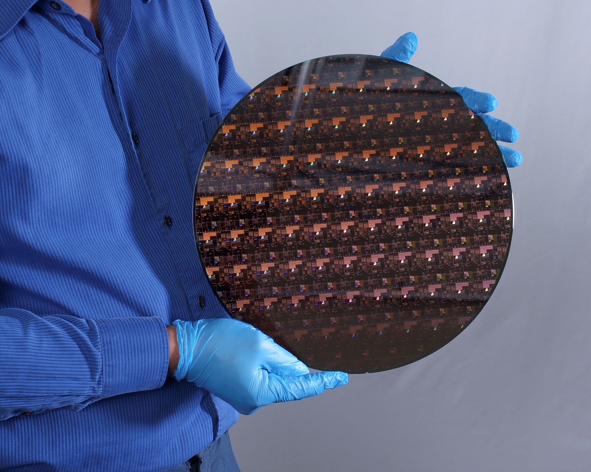
In today's digital age, the most widespread application of transistors is in computer memory chips and microprocessors, making the study and understanding of transistor technology more vital than ever.
What is a transistor?
Transistors serve as the active components within a computer chip (also referred to as a microchip, integrated circuit, or IC). These chips can house billions of transistors, etched onto their gleaming surfaces. Within the chip, transistors function as interconnected miniature electrical switches. They are responsible for amplifying electrical signals or regulating the flow of electric current – turning it on or off.
Akin to any electrical switch, a transistor performs three essential functions. Firstly, when switched on, it should allow the maximum amount of current to flow through. Secondly, when turned off, it should permit little to no current leakage. Lastly, for optimal performance, it needs to switch on and off at high speed.
In essence, each transistor is capable of representing two states, thus storing two distinct values – zero and one. Given the fact that a chip can host billions of transistors, it means that a single chip can hold and process a staggering number of zeros and ones. This allows the chip to send, receive, and process an impressive volume of data, which underscores the significance of transistors in the world of data processing and electronics.
History of the transistor
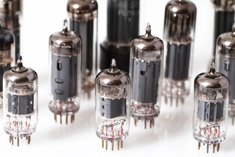
In the 1940s, vacuum tubes and electromechanical relays were widely used in the quickly growing telephone networks. Electromechanical relays had made fully automatic telephone dialing and switching a reality, but the relays had low speeds.
Vacuum tubes were widely used as diodes and triodes in the electronics industry of the time. The first computer that would use vacuum tubes, the Electronic Numerical Integrator and Computer, also known as ENIAC, was built in 1946. In fact, the ENIAC used more than 17 000 vacuum tubes for its operation, allowing signals to be sent and calculations to be performed more quickly through the use of electrical switching rather than the slower mechanical switching.
The problem with vacuum tubes was that they were not very dependable, and they were huge compared to transistors – as a consequence, the ENIAC occupied a 15x9 meter (50x30 foot) large room. It processed about 500 floating point operations per second (FLOPS). The theoretical performance of Apple's M2 processor in its latest iPhones is rated at 3.6 Teraflops, i.e., 3.6 trillion FLOPS – and it fits on a fingernail.
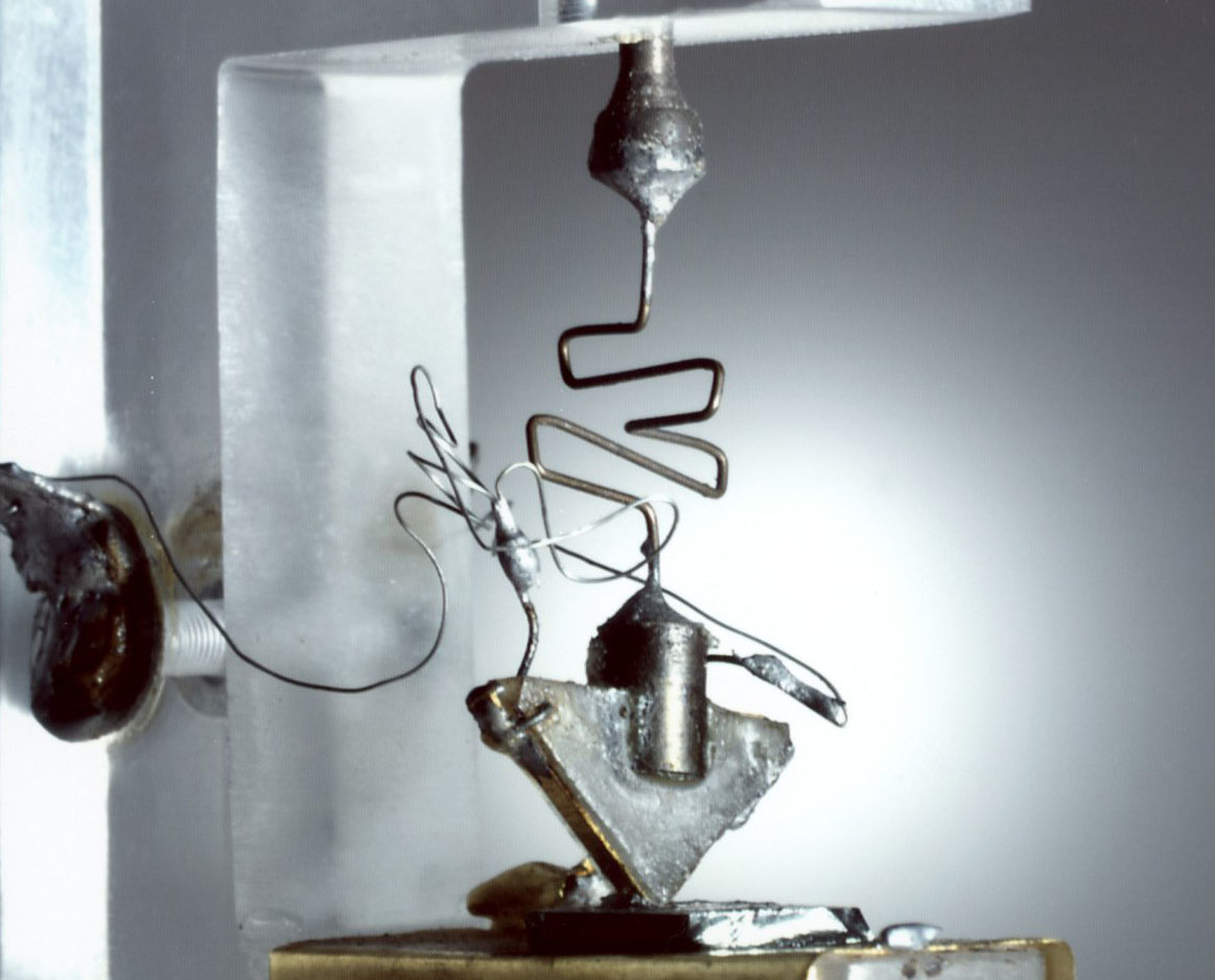
In the 1940s at Bell Labs in Murray Hill, New Jersey, physicists John Bardeen, Walter Brattain, and William Shockley set about studying semiconductor materials to see whether they could create a durable alternative that might eventually replace vacuum tubes in telephone networks.
Bardeen, Brattain and Shockley had tested various combinations of p-type and n-type semiconductors under different conditions until they finally found a configuration that would allow a thin layer of semiconductor to regulate a large flow of current between two electrodes.
On December 16, 1947, they demonstrated the first working transistor, now known as the point-contact transistor (a feat for which they were awarded the 1956 Nobel Prize in Physics). The first transistor was roughly the size of a thumb.
Although the point-contact transistor was the first transistor invented, it never succeeded commercially because hard-to-control variations in the metal-to-semiconductor point contacts made it difficult to manufacture them reliably and with uniform operating characteristics.
Commercial transistors started to take off after in July 1951, Bell Labs announced the successful invention and development of the junction transistor.
By the end of the 1950s, bipolar junction transistors had almost completely replaced electron tubes in computer applications.
The transistor worked more efficiently than the vacuum tube and operated on less power. Not only did this revolutionize telephone networks and computer technology, but it also allowed computers to become smaller and more cost-effective and advance at a faster pace. Transistors became the steppingstone between vacuum tubes and modern computer technology.
The year 1971 saw the advent of the first microprocessor: Intel's 4004, incorporating 2,300 transistors and the first memory. The Intel 4004 microprocessor circuit line width was 10 microns, or 10,000 nanometers. 40 years later, an Intel Core processor with a 32 nm processing die held 560 million transistors. Another 10 years later, by 2021, the top-of-the-line M2 processors used by Apple are chips built with 5-nm technology that contain 20 billion transistors.
The complexity of integrated circuits has grown exponentially, doubling every 2 to 3 years according to Moore's law, as transistors continue to become increasingly miniaturized.
Moore's Law, postulated by Intel's co-founder Gordon Moore in 1965, observes the empirical regularity that the number of transistors on integrated circuits doubles approximately every two years. This observation has held for more than 50 years now and drives the progress in computing such as the processing speed and the price of computers.
How do transistors work?
A transistor, integral to virtually all modern electronic devices, is a device designed to control, amplify, and generate electrical signals. Its operational efficacy relies on the electronic properties of a semiconductor material. It helps regulate or control the flow of current or voltage, acting as a switch or gate, thereby amplifying and generating electrical signals.
Operating primarily as an electronic switch, a transistor can turn a current ON and OFF. This operational principle is key to processing binary code (0 signifies blocked current, 1 allows current to pass through) in logic circuits including inverters, gates, adders, and memory cells. Furthermore, a transistor can also be partially turned on, a feature crucial to building amplifiers.
The role of semiconductors
Semiconductors play a pivotal role in this context. Contrary to conductors like metals, which have a plethora of free electrons to carry an electric current, semiconductors like silicon and germanium host very few charge carriers. However, the introduction of minute quantities of certain impurities, through a process called doping, can alter the number of charge carriers. Doping modulates the electrical, optical, and structural properties of the semiconductor, thus enabling silicon to acquire free electrons that carry electric current.
Post-doping, the semiconductor is referred to as an extrinsic semiconductor, whereas its pure, undoped form is an intrinsic semiconductor. Silicon semiconductors are classified into two categories based on the type of impurity used for doping: n-type, where electrons flow out, and p-type, where electrons flow in. Regardless of the type, the semiconductor allows the transistor to function as a switch or amplifier.
n-type and p-type transistors
For instance, doping silicon with a small amount of phosphorus or arsenic creates an n-type semiconductor, with the electrons donated by the phosphorus or arsenic acting as charge carriers. On the other hand, doping silicon with boron or gallium results in a p-type semiconductor. In this case, boron or gallium offers a positively charged carrier by removing an electron from silicon, leaving behind a hole that acts as a carrier of positive charge.
The significance of semiconductors arises from the interaction between electrons and holes. The major distinction between n- and p-type doping lies in the direction of electron flow through the deposited layers of the semiconductor. Both n- and p-type silicon function as decent conductors of electricity. Alone, neither n- nor p-type silicon is particularly outstanding. However, when they are combined, intriguing behavior is observed at the junction between the two.
This behavior at the p-n junction, the interface between two dissimilar layers, heavily influences the operation of junction transistors and most other semiconductor devices. Understanding these operations is key to understanding how transistors work and contribute to the complex world of electronics.
What types of transistors are there?
Transistor design has evolved over time, from planar to FinFET to gate-all-around (GAA) transistors.
BJT, MOSFET and OFET
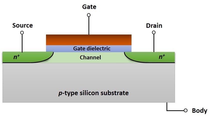
Typically, a transistor – which is based on the transport of electrons in a solid (i.e., a solid-state device) and not in a vacuum, as in the vacuum tubes of old – consists of at least three terminals for connection to an electronic circuit: the base, the emitter, and the collector, as they are called in the classical bipolar junction transistor (BJT). In modern switching applications that use field effect transistors (FETs), they are called the gate, the drain, and the source.
The source acts as the emitter filament of an electron tube; the drain acts as the collector plate; and the gate acts as controller. These elements work differently in the two main types of transistor used today: bipolar junction transistors, which came first, and the metal-oxide-semiconductor field-effect transistor (MOSFET).
When working as an amplifier, a transistor transforms a small input current into a bigger output current. As a switch, it can be in one of two distinct states – ON or OFF – to control the flow of electronic signals through an electrical circuit or electronic device.
Today, MOSFETs are the most common type of transistor. This is due to the unique features of this transistor, mainly low-power consumption and high manufacturing yield. It can be used as a switch and also to amplify signals in electronic devices.
Organic field-effect transistors (OFETs) are a type of transistor that uses an organic semiconductor material as the active layer. Unlike conventional transistors that rely on inorganic semiconductors like silicon, OFETs leverage the unique properties of organic materials to enable novel applications in flexible, printable, and low-cost electronics.
Transistor designs
Planar transistors
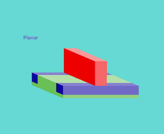
This design is the classical bipolar junction transistor (so called because it has two p-n junctions) that brings key elements of a transistor on a two-dimensional plane, including the gate, which modulates conductivity through a channel, the source, through which drive current enters the channel, and the drain, where current leaves the channel.
The types of bipolar junction transistor are n-p-n and p-n-p transistors. The n-p-n transistor is made by placing a p-type material between two n-type materials. The p-n-p transistor is made by placing an n-type material between two p-type materials.
All these components are built on a base of the semiconducting material silicon. This transistor concept was industrialized in the 1950s and 60s and was highly suited for mass production and miniaturization.
FinFET transistors

Over time, engineers discovered that it's possible to exert more control over the flow of current in the channel by raising the gate above the plane of the silicon, like a fin above water. Whereas the bipolar junction transistor is current controlled, the field-effect transistor (FET) is voltage controlled. Also, the FET is a unipolar device, which means that it is made using either p-type or n-type material as main substrate. Hence the current conduction of a FET is done by either electrons or holes.
The main advantage of a FET is that it has a very high input impedance, which is in the order of mega Ohms. Additional advantages are low power consumption, low heat dissipation - making FETs highly efficient devices. Consequently, the industry made the switch from 2D planar transistors to 3D fin field-effect transistors, abbreviated as FinFETs.
In FinFET transistors, the gate wraps around the channel on three sides of a silicon fin, as opposed to across its top as in planar transistors. This creates an inversion layer with a much larger surface area, which allows the gate to better control the flow of current through the transistor. This means that more current can flow through with less leakage, and a lower gate voltage is needed to operate the transistor. In addition, the vertical geometry of FinFETs made it possible for engineers to pack more transistors in a chip, advancing Moore's Law even further. The result was a chip with better performance, lower power consumption and a leading status through the 2010s.
Tunnel field-effect transistors (TFETs)
Tunnel field-effect transistors are a type of transistor that utilize quantum tunneling to enable ultralow-power operation. In a TFET, the source and drain regions have opposite doping types, forming a p-i-n structure. When a voltage is applied to the gate, the energy bands in the channel region are modulated, allowing electrons to tunnel from the valence band of the source to the conduction band of the drain. This band-to-band tunneling mechanism allows TFETs to achieve a steep subthreshold slope, enabling them to be switched on and off with a very small change in gate voltage. As a result, TFETs have the potential to greatly reduce the power consumption of electronic devices compared to conventional MOSFETs. However, manufacturing challenges and relatively low on-state currents have limited their widespread adoption so far.
Gate-all-around transistors

With the state-of-the-art chip nodes that the leading chip manufacturers are manufacturing, FinFETs are reaching the limit of how high fins can go and how many fins can be placed side by side to boost their current-carrying capacity without suffering from electrical challenges.
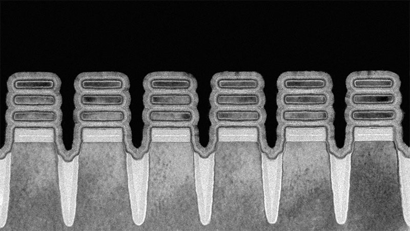
To further improve the control of the transistor channel, engineers found a way to replace the vertical fin with a stack of horizontal sheets, creating a new concept called gate-all-around field-effect transistors, which are shortened to GAA transistors, or GAAFETs.
Gate-all-around transistors use stacked nanosheets. These separate horizontal sheets are vertically stacked so that the gate surrounds the channel on all four sides, further reducing leakage and increasing drive current. This means superior electrical signals pass through and between the transistors, improving chip performance.
Additionally, chipmakers now have the flexibility to vary the width of the nanosheets to best suit a particular chip design. Specifically, wide nanosheets allow for higher and better drive current, while narrow nanosheets can optimize power consumption.
How transistors are made
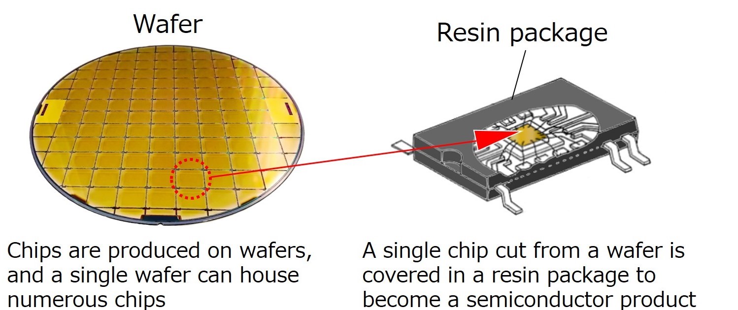
The transistors on microchips are made by building up layers of interconnected patterns on a silicon wafer. This manufacturing process is a highly intricate undertaking involving hundreds of high-precision steps undertaken in ultra-clean rooms with complex and specialized machinery.
Since their early days, transistors were made with silicon (Si), which remains the most widely used semiconductor due to the exceptional quality of the interface created by silicon and silicon oxide (SiO2), which serves as an insulator.
Here is a summarized overview of the key steps:
1) Deposition
The first step in creating a microchip is typically to deposit thin films of materials onto the silicon wafer. These materials can be conductors, isolators or semiconductors.
2) Lithography
Lithography, or photolithography, is the critical step in the computer chip-making process. It involves coating the wafer with photosensitive material and exposing it with light inside a lithography machine.
3) Photoresist coating
To print a layer of a chip, the wafer is first coated with a light-sensitive layer called a 'photoresist', or 'resist', for short. It then enters the lithography machine.
4) Exposure
Inside the lithography machine, light is projected onto the wafer through the reticle containing the blueprint of the pattern to be printed. The system's optics shrink and focus the pattern onto the resist. Where light hits the resist, it causes chemical changes, recreating the pattern from the reticle in the resist.
5) Computational lithography
The reticle containing the pattern to be printed on the wafer sometimes needs to be optimized by intentionally deforming the pattern to compensate for physical and chemical effects that occur during lithography.
6) Baking and developing
After leaving the lithography machine, the wafer is baked and developed to make those changes permanent, and some of the photoresist is washed away to create a pattern of open spaces in the resist.
7) Etching
Materials such as gases are used to etch away material from the open spaces creating during the developing phase, leaving a 3D version of the pattern.
8) Metrology and inspection
Throughout the chip production process, the wafer is measured and inspected for errors. These measurements are fed back to the systems and are used to optimize and stabilize the equipment.
9) Ion implantation
The wafer may also be bombarded with positive or negative ions to tune the semiconductor properties of parts of the pattern before the remaining photoresist is removed.
10) Repeat, repeat, repeat
Steps 1-9, from deposition to resist removal, is repeated until the wafer is covered in patterns, completing one layer of the wafer's chips. To make an entire chip, this process can be repeated up to 100 times, laying patterns on top of patterns to create an integrated circuit.
11) Processed wafer
In the final step in production, the wafer is diced into individual chips, which are encapsulated in protective packages.
There is an excellent map of the manufacturing process, from the initial growth of a silicon oxide film all the way to the final wiring layer generation processes here at the Toshiba website.
Who makes transistors?
Transistors are manufactured by a variety of companies, including large multinational corporations as well as smaller specialty firms. Some of the leading manufacturers of transistors include:
- Intel
- Samsung
- TSMC (Taiwan Semiconductor Manufacturing Company)
- SK Hynix
- Qualcomm
- Broadcom
- Texas Instruments
- ON Semiconductor
These companies use a variety of materials and processes to manufacture transistors, including silicon, germanium, and other semiconductor materials. They may also produce different types of transistors, such as bipolar transistors, metal-oxide-semiconductor field-effect transistors (MOSFETs), and other types of devices. Many of these companies also design and manufacture other types of semiconductor devices, such as integrated circuits, memory chips, and sensors.
Taiwan Semiconductor Manufacturing Co. (which produces all of Apple's chips), Intel and Samsung Electronics are the only companies that can manufacture the most advanced microchips. The reason this club is so exclusive is the immense capital cost of building semiconductor fabrication plants (fabs or foundries) that produce these chips. For instance, TSMC is reportedly spending $34 billion on its latest foundry that will make future 2 nm chips.
However, these fabs couldn't exist on their own. The advanced semiconductor industry is an intricate network of specialist companies from America, Europe and Asia.
Just to give you an idea of this ecosystem: Using sophisticated computer-aided design tools and software from Synopsys and Cadence, companies like AMD, Qualcomm, Intel, Apple and Nvidia excel at the design of the most advanced chips. Applied Materials develops and manufactures equipment used in various steps of the wafer fabrication process. ASML provides lithography. Zeiss SMT specializes in optical lenses, which draws the stencils on the silicon wafers from those designs, using both deep and extreme ultraviolet light. Lam Research, KLA and other firms provide various sophisticated and highly specialized wafer fabrication equipment.
Frequently Asked Questions (FAQs) About Transistors
What is a transistor?
A transistor is a type of semiconductor device that is used to amplify or switch electronic signals and electrical power. It is a fundamental building block of modern electronic devices and is commonly used in devices such as radios, televisions, and computers.
The transistor was invented by a team of three scientists at Bell Laboratories in the United States in 1947. The inventors were John Bardeen, Walter Brattain, and William Shockley.
How do transistors work?
Transistors work by using a small amount of electrical current to control a larger current. This is accomplished by using two types of semiconductor material, called "p-type" and "n-type". The different types of material are arranged in three layers, with the p-type in the middle for a typical transistor. When voltage is applied to the middle layer (called the "base"), it allows current to flow from the outer "emitter" layer to the other outer "collector" layer.
What are the different types of transistors?
There are two basic types of transistors: Bipolar Junction Transistors (BJTs) and Field Effect Transistors (FETs). BJTs are controlled by current, while FETs are controlled by voltage. Within these categories, there are further subdivisions such as NPN and PNP BJTs and N-Channel and P-Channel MOSFETs.
What is a MOSFET transistor?
MOSFET stands for Metal Oxide Semiconductor Field Effect Transistor. It is a type of transistor that uses an electric field to control the electrical behavior of the device. MOSFETs are particularly useful for their high-speed switching capabilities and are widely used in digital circuits.
What is a transistor used for?
Transistors are used in a wide variety of applications. They can act as amplifiers, taking a small input signal and making it larger. They can also be used as switches, turning an electrical signal on or off. You will find transistors in nearly every modern electronic device, from mobile phones and computers to radios and amplifiers.
How are transistors made?
Transistors are made using a complex process called photolithography. This involves creating a pattern on a silicon wafer using a process similar to photography. The pattern is then used to guide the placement of the different types of semiconductor material.
What does "NPN" or "PNP" mean in terms of a transistor?
"NPN" and "PNP" refer to the arrangement of the different types of semiconductor material in a Bipolar Junction Transistor (BJT). In an NPN transistor, there's a layer of p-type semiconductor material sandwiched between two layers of n-type material. In a PNP transistor, the arrangement is reversed, with a layer of n-type material between two layers of p-type material.
How do you know if a transistor is bad or failing?
Typical signs of a failing transistor include a circuit that's not functioning as expected, or a device that's overheating or not powering on. To confirm, you can use a multimeter to test the transistor. If the transistor isn't showing the correct voltages or resistances in its different configurations, it's likely that it's bad.
What is transistor biasing?
Transistor biasing is the process of setting a predetermined amount of current or voltage at the junction of a transistor to allow it to operate in a certain region of its output characteristics. This allows the transistor to function as an amplifier, a switch, or other device. Different types of biasing techniques exist, such as fixed bias, collector to base bias, and voltage divider bias.
