Organic Field-Effect Transistors: The Future of Flexible Electronics
What are Organic Field-Effect Transistors?
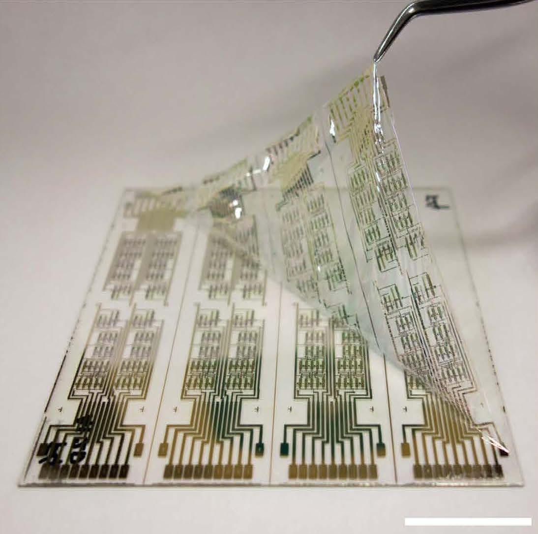
Organic field-effect transistors (OFETs) are a type of transistor that uses an organic semiconductor material as the active layer. Unlike conventional transistors that rely on inorganic semiconductors like silicon, OFETs leverage the unique properties of organic materials to enable novel applications in flexible, printable, and low-cost electronics.
Key Components of OFETs
An OFET consists of several key components:
- Organic Semiconductor Layer: This is the active layer of the transistor, responsible for charge transport. It is typically made of conjugated organic molecules or polymers that exhibit semiconducting properties.
- Gate Electrode: The gate electrode controls the conductivity of the organic semiconductor layer. When a voltage is applied to the gate, it induces an electric field that modulates the charge carrier density in the semiconductor.
- Source and Drain Electrodes: These electrodes are responsible for injecting and collecting charge carriers (electrons or holes) in the organic semiconductor layer. The flow of charge carriers between the source and drain is controlled by the gate voltage.
- Dielectric Layer: The dielectric layer separates the gate electrode from the organic semiconductor. It plays a crucial role in determining the performance of the OFET, as it affects the capacitance and the gate-induced electric field.
Fabrication Methods of OFETs
OFETs can be fabricated using various methods, depending on the materials, substrates, and desired device characteristics. Some common fabrication techniques include:
Solution Processing
Solution processing is a widely used method for fabricating OFETs, as it allows for low-cost, large-area, and high-throughput production. Organic semiconductors are dissolved in a suitable solvent and deposited onto the substrate using techniques such as spin coating, inkjet printing, or blade coating. The solvent evaporates, leaving a thin film of the organic semiconductor on the substrate.
Vacuum Deposition
Vacuum deposition techniques, such as thermal evaporation and organic vapor phase deposition (OVPD), can be used to fabricate OFETs with high purity and precision. In these methods, the organic semiconductor is heated in a vacuum chamber, and the vaporized molecules are deposited onto the substrate. Vacuum deposition allows for the fabrication of multilayer structures and the control of film thickness and morphology.
Printing Techniques
Printing techniques, such as screen printing, gravure printing, and flexographic printing, are attractive for the large-scale production of OFETs on flexible substrates. These methods involve the transfer of the organic semiconductor ink onto the substrate through a patterned mask or a textured roller. Printing techniques enable the fabrication of OFETs with complex patterns and high resolution.
Self-Assembly
Self-assembly is an emerging approach for the fabrication of OFETs, where the organic semiconductor molecules spontaneously organize into ordered structures on the substrate. This can be achieved through various methods, such as solution-based self-assembly, Langmuir-Blodgett deposition, or surface-initiated polymerization. Self-assembly allows for the precise control of the molecular arrangement and can lead to improved charge transport properties.
The choice of fabrication method depends on factors such as the desired device performance, the compatibility of materials, the substrate properties, and the scalability and cost-effectiveness of the process. Researchers are continuously exploring new fabrication techniques and optimizing existing methods to improve the performance and reliability of OFETs.
Advantages of OFETs
OFETs offer several advantages over conventional inorganic transistors:
- Flexibility: Organic semiconductors can be deposited on flexible substrates, enabling the fabrication of stretchable and flexible electronic devices. This opens up new possibilities for wearable electronics, flexible displays, and conformable sensors.
- Low-Cost Processing: OFETs can be manufactured using solution-based processes, such as inkjet printing, spin coating, and roll-to-roll processing. These techniques are less expensive and more scalable compared to the high-temperature, vacuum-based processes used for inorganic transistors.
- Tunable Properties: The properties of organic semiconductors can be tailored through chemical synthesis and molecular design. This allows for the optimization of charge transport, optical properties, and other functionalities to suit specific applications.
Applications of OFETs
OFETs have a wide range of potential applications in various fields:
Flexible Displays
OFETs can be used as switching elements in flexible displays, such as organic light-emitting diode (OLED) displays and electronic paper (e-paper). The flexibility and low-cost processing of OFETs enable the development of rollable, foldable, and conformable displays for mobile devices, smart watches, and other consumer electronics.
Wearable Electronics
OFETs are promising candidates for wearable electronics applications, such as health monitoring devices, smart textiles, and conformable sensors. The flexibility and biocompatibility of organic materials make them suitable for integration with clothing, skin, and other soft surfaces.
Sensor Applications
OFETs can be used as chemical and biological sensors, leveraging the sensitivity of organic semiconductors to various analytes. By functionalizing the semiconductor layer or incorporating specific receptors, OFETs can detect gases, organic compounds, and biomolecules with high sensitivity and selectivity.
Neuromorphic Computing
OFETs have shown promise in neuromorphic computing, which aims to emulate the functionality of biological neural networks. The inherent nonlinearity and plasticity of organic semiconductors can be exploited to develop artificial synapses and neurons for brain-inspired computing systems.
Challenges and Future Perspectives
Despite the significant progress in OFET technology, several challenges remain to be addressed. One of the main challenges is improving the charge carrier mobility and stability of organic semiconductors to achieve higher performance and longer device lifetimes. Researchers are exploring new materials, device architectures, and processing techniques to overcome these limitations.
Another challenge is the integration of OFETs with other electronic components, such as sensors, memories, and power sources, to create fully functional organic electronic systems. The development of standardized manufacturing processes and the optimization of device interfaces are crucial for the successful integration of OFETs into practical applications.
Future research in OFETs will focus on the development of high-performance organic semiconductors, the exploration of novel device architectures, and the integration of OFETs with other emerging technologies, such as printed electronics, energy harvesting, and biosensors. The combination of OFETs with machine learning algorithms and neuromorphic computing approaches will also open up new opportunities for intelligent and adaptive organic electronic systems.
Further Reading
Different Types of Field-Effect Transistors - Theory and Applications, Organic Field-Effect Transistor: Device Physics, Materials, and Process
npj Flexible Electronics, Advances in flexible organic field-effect transistors and their applications for flexible electronics
