Transition Metal Dichalcogenides (TMDs) – A Promising Class of 2D Materials for Advanced Technologies
Contents
Key Takeaways About Transition Metal Dichalcogenides
- Definition: TMDs are layered 2D nanomaterials with the formula MX₂, where M is a transition metal (Mo, W, etc.) and X is a chalcogen (S, Se, Te)
- Unique Properties: They feature tunable direct bandgaps, exceptional exciton binding energies, strong light-matter interactions, and valley-selective optical responses
- Electronic Behavior: TMDs transition from indirect bandgap in bulk to direct bandgap in monolayer form, enabling efficient light emission and absorption
- Structural Versatility: Their phase can be switched between semiconducting (2H) and metallic (1T) states, allowing for multiple functionalities within the same material
- Applications: TMDs are promising for flexible electronics, optoelectronics, quantum computing, energy storage, photovoltaics, and sensing devices
- Heterostructures: When layered with other 2D materials, TMDs form van der Waals heterostructures with engineered properties and enhanced functionalities
- Challenges: Scalable synthesis with consistent quality, environmental stability, and reliable integration into commercial devices remain hurdles for widespread adoption
Introduction to Transition Metal Dichalcogenides
Transition metal dichalcogenides (TMDs) represent one of the most promising families of two-dimensional (2D) nanomaterials in advanced materials research. Characterized by their MX₂ formula—where M denotes transition metals like molybdenum (Mo), tungsten (W), or titanium (Ti), and X represents chalcogen elements such as sulfur (S), selenium (Se), or tellurium (Te)—TMDs have emerged as frontrunners in next-generation semiconductor technology.
Since the groundbreaking isolation of graphene in 2004, the field of 2D materials has expanded dramatically, with TMDs now at the forefront of quantum materials engineering. These atomically thin semiconductors exhibit exceptional properties including tunable direct bandgaps, high carrier mobility, strong light-matter interactions, and mechanical flexibility—characteristics that silicon-based technologies cannot match at nanoscale dimensions.
Recent breakthroughs in large-scale synthesis techniques and heterostructure engineering have accelerated TMD integration into practical applications. From ultra-efficient field-effect transistors (FETs) and flexible optoelectronic devices to quantum computing components and sustainable energy storage systems, TMDs are transforming multiple technology sectors simultaneously. Their unique valley-dependent physics and spin-orbit coupling also make them invaluable for spintronics and valleytronics research.
This comprehensive guide explores the fundamental structure, extraordinary properties, synthesis methods, and emerging applications of transition metal dichalcogenides—materials that are redefining the boundaries of nanoscience and enabling technologies previously thought impossible.
Structure and Properties of Transition Metal Dichalcogenides
Crystal Structure and Atomic Arrangement
TMDs possess a layered structure represented by the formula MX2, where M is a transition metal atom (Group 4-10 elements such as Mo, W, Ti, Zr, Hf, V, Nb, Ta) and X is a chalcogen atom (S, Se, or Te). Each monolayer consists of a hexagonally arranged transition metal layer sandwiched between two chalcogen layers in either trigonal prismatic (2H phase, most common in semiconducting TMDs) or octahedral coordination (1T phase, common in metallic TMDs).
The intralayer M-X bonds are predominantly covalent, while adjacent layers are held together by relatively weak van der Waals forces, enabling mechanical exfoliation. This structural feature leads to a significant interlayer distance of approximately 6.5 Å, which varies slightly depending on the specific TMD composition.
Electronic Properties and Bandgap Engineering
The electronic properties of TMDs vary dramatically with composition, number of layers, strain, and phase. Most Group 6 TMDs (Mo, W-based) exhibit semiconductor behavior with bandgaps in the range of 1-2 eV, while Group 4 and 5 TMDs often display metallic or semimetallic characteristics.
A defining feature of semiconducting TMDs is their layer-dependent band structure. Bulk TMDs typically possess indirect bandgaps (e.g., 1.2 eV for bulk MoS2), but remarkably transition to direct bandgaps when thinned to the monolayer limit (e.g., 1.8 eV for monolayer MoS2). This transition occurs because quantum confinement affects the bands at the Γ and K points differently. At the monolayer limit, the valence band maximum and conduction band minimum both occur at the K points of the Brillouin zone, creating a direct bandgap that enables efficient light emission and absorption.
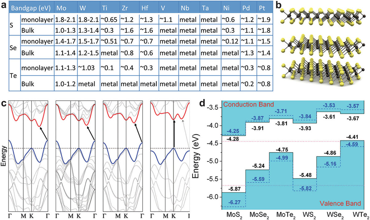
Two-dimensional transition metal dichalcogenides (2D-TMDs). (a) The table shows common TMDs and their band gap. (b) A schematic illustration of the layered structure of MoS2. (c) Energy dispersion in bulk, quadrilayer (4L), bilayer (2L) and monolayer (1L) MoS2 from left to right. The horizontal dashed line represents the energy of a band maximum at the K point. The red and blue lines represent the conduction and valence band edges, respectively. The lowest energy transition increases with the decreasing layer and evolve from indirect to direct (vertical) transitions. (d) The relative valence and conduction band edge of some common TMDs (monolayer).(© The Royal Society of Chemistry) (click on image to enlarge)
Optical Properties and Excitonics
The direct bandgap nature of monolayer TMDs leads to exceptional optical properties, characterized by strong light-matter interactions. These materials exhibit remarkably high absorption coefficients despite being atomically thin, absorbing up to 15% of incident light per monolayer.
One of the most distinctive features of TMDs is their exceptionally strong excitonic effects. Due to reduced dielectric screening and quantum confinement, exciton binding energies in monolayer TMDs range from 0.3 to 0.7 eV—orders of magnitude higher than conventional semiconductors like silicon or GaAs. This results in stable excitons observable even at room temperature, making TMDs excellent candidates for excitonic devices.
The optical response of TMDs also exhibits unique valley-selective circular dichroism, where specific valleys in the band structure can be selectively excited by circularly polarized light. This valley-dependent optical selection rule arises from the broken inversion symmetry and strong spin-orbit coupling, enabling potential applications in valleytronics and quantum information processing.
Mechanical and Thermal Properties
Despite their atomic thinness, TMDs display remarkable mechanical properties. Monolayer MoS2, for example, exhibits a Young's modulus of approximately 270 GPa and can withstand significant strain before breaking. These properties, combined with their flexibility, make TMDs particularly suitable for flexible and stretchable electronics.
The thermal conductivity of TMD monolayers is typically lower than graphene but comparable to bulk silicon. This anisotropic thermal behavior, with conductivity primarily along the in-plane direction, has implications for thermal management in TMD-based nanoelectronics.
Defects and Phase Engineering
Point defects (vacancies, antisite defects), line defects (grain boundaries), and edge states play crucial roles in determining the electronic, optical, and catalytic properties of TMDs. Chalcogen vacancies are the most common point defects, introducing mid-gap states that can significantly alter electronic transport and optical response.
TMDs can exist in multiple phases with different electronic properties. The semiconductor 2H phase (trigonal prismatic coordination) can be transformed to the metallic 1T phase (octahedral coordination) through chemical, electrical, or mechanical methods. This phase engineering enables remarkable functionalities such as low-resistance contacts, enhanced catalysis, and improved energy storage performance.
Van der Waals Heterostructures and Applications
The van der Waals interactions between neighboring layers of TMDs enable more flexible integration of different materials without lattice matching limitations, creating vast possibilities for controlling various properties at the atomic scale. These structures are called van der Waals heterostructures.
Due to their extraordinary optical and electrical properties, 2D TMDs have emerged as a promising class of atomically thin semiconductors for next-generation electronic and optoelectronic devices. For example, their optical properties could make computers run a million times faster and store information with a million times more energy efficiency.
Electronic and Optoelectronic Devices Based on 2D TMDs
Early research in 2D-TMDs has focused on their potential as a new generation of atomically thin semiconductors for functional electronics and optoelectronics. In 2013, researchers demonstrated the first n-type field-effect-transistor (FET) made of a monolayer of tungsten diselenide (WSe2), showcasing the material's potential for future low-power and high-performance integrated circuits.
With intrinsic bandgaps typically in the 1-2 eV range, 2D-TMDs overcome graphene's key shortcomings for electronic applications, making them ideal for use in transistors. Additionally, TMDs have excellent absorption properties for circularly polarized light, making them suitable for use in detectors.
Synthesis of Atomically Thin 2D Transition Metal Dichalcogenides
Initial TMD research and device demonstrations often relied on exfoliated flakes, which limited the flake size to around 10 µm or less. This led to the fabrication of 2D-TMD heterostructure devices through labor-intensive exfoliation and repeated physical transfer processes, an approach not scalable for practical technologies.
To fully explore TMD potential, researchers have developed two distinct synthetic strategies: top-down approaches, including mechanical, chemical, and solvent exfoliation; and bottom-up strategies, which involve chemical synthesis of atomically thin nanosheets in solution phase or through chemical vapor deposition processes.
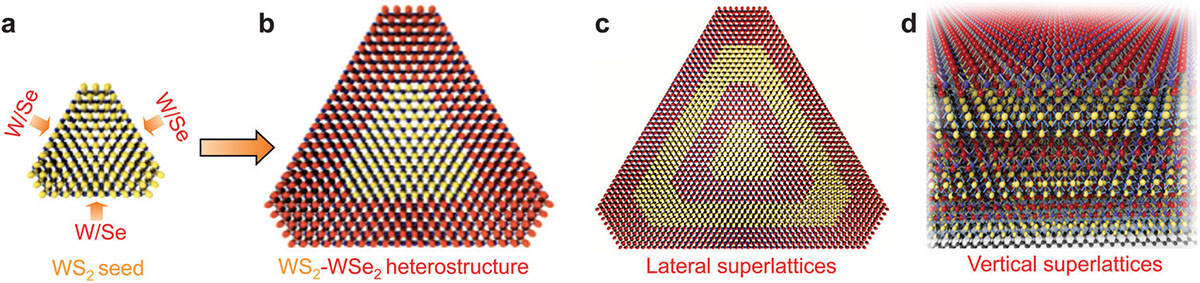
Growth of 2D-TMD heterostructures. (a and b) A schematic illustration of lateral epitaxial growth of WS2–WSe2 heterostructures. (c) A schematic illustration of successive lateral epitaxial growth of superlattice structure in the lateral dimension. (d) A schematic illustration of van der Waals superlattices through the successive layer-by-layer growth approach. (© The Royal Society of Chemistry) (click on image to enlarge)
Future Outlook: The Road Ahead for TMD Research and Applications
The extraordinary properties of transition metal dichalcogenides have positioned them at the forefront of materials science and nanotechnology research. As we've explored throughout this article, TMDs offer a unique combination of electronic versatility, optical responsiveness, and mechanical flexibility that opens doors to technologies beyond the capabilities of conventional semiconductors.
Current research is rapidly advancing on multiple fronts. Scalable synthesis methods are evolving from laboratory curiosities to industrial processes, with recent breakthroughs in chemical vapor deposition enabling wafer-scale production of high-quality TMD films. Simultaneously, defect engineering approaches are transforming what were once viewed as material imperfections into valuable tools for property tuning and functionality enhancement.
The integration of TMDs with other emerging materials—from graphene to topological insulators—continues to expand the horizon of what's possible in device engineering. These heterostructures, precisely assembled layer by layer, represent a new paradigm in materials design where properties can be crafted with atomic precision.
Looking ahead, several key developments are likely to shape the field:
First, the commercialization of TMD-based technologies will accelerate as manufacturing challenges are overcome. We can expect to see TMDs appearing in specialized electronics, particularly where flexibility, optical sensing, or operation in extreme environments is required.
Second, quantum applications of TMDs will gain prominence as researchers harness their valley physics and strong spin-orbit coupling for quantum information processing. The unique ability to access and manipulate quantum degrees of freedom in these materials at room temperature gives them significant advantages over many competing quantum platforms.
Third, energy applications—from photovoltaics to catalysis—will benefit from continued optimization of TMD properties. Their high surface-to-volume ratio, tunable electronic structure, and abundant active sites make them promising candidates for addressing critical energy challenges.
While significant challenges remain, particularly in large-scale production consistency and long-term device stability, the trajectory of TMD research suggests these atomically thin materials will have an outsized impact on next-generation technologies. As the boundaries between fundamental research and practical applications continue to blur, transition metal dichalcogenides stand ready to transform from laboratory marvels to key components in tomorrow's technological landscape.
For further reading, we recommend this article in Nature Reviews Materials: "2D transition metal dichalcogenides".
Frequently Asked Questions (FAQs) about Transition Metal Dichalcogenides (TMDs)
What are Transition Metal Dichalcogenides?
Transition Metal Dichalcogenides (TMDs) are a type of layered material, formed from one of the transition metals and either sulfur, selenium or tellurium - the chalcogens. The layer structure of these materials allows them to possess unique electronic, optical, and mechanical properties, which makes them interesting for a wide range of applications, from nanoelectronics to energy storage.
What are the key properties of Transition Metal Dichalcogenides?
TMDs are known for their semiconducting properties, high surface-to-volume ratio, strong light-matter interaction, and mechanical flexibility. The electrical and optical properties can also be modified by changing the number of layers, making them versatile materials for device engineering.
Why are the excitonic properties of TMDs considered exceptional?
TMDs exhibit remarkably strong excitonic effects due to reduced dielectric screening and quantum confinement in their 2D structure. Their exciton binding energies (0.3-0.7 eV) are orders of magnitude higher than conventional semiconductors, allowing excitons to remain stable at room temperature. This enables efficient light emission and absorption, making TMDs promising for optoelectronic applications like LEDs, photodetectors, and optical sensors.
What is valleytronics and how do TMDs enable it?
Valleytronics is an emerging field that utilizes the valley degree of freedom in semiconductors for information processing and storage. TMDs are ideal for valleytronics because their hexagonal lattice structure creates distinct "valleys" in their electronic band structure at the K and K' points of the Brillouin zone. Due to broken inversion symmetry and strong spin-orbit coupling, these valleys can be selectively excited with circularly polarized light, allowing for valley-specific information manipulation that could lead to new types of quantum devices.
What applications do Transition Metal Dichalcogenides have?
TMDs are being studied for use in a variety of fields, including electronics, optoelectronics, energy storage, catalysis, and sensors. Their high surface-to-volume ratio makes them excellent for applications in catalysis and energy storage, while their tunable bandgap and high carrier mobility make them suitable for electronics and optoelectronics.
How are Transition Metal Dichalcogenides synthesized?
TMDs can be synthesized through several approaches: top-down methods like mechanical and chemical exfoliation from bulk crystals, and bottom-up methods including chemical vapor deposition (CVD), physical vapor deposition (PVD), and atomic layer deposition (ALD). While lab-scale production is well-established, scalable industrial synthesis with consistent quality and yield remains challenging. Recent advances in CVD techniques are making wafer-scale production more feasible.
What is phase engineering in TMDs and why is it important?
Phase engineering refers to the controlled transformation between different crystalline phases of TMDs, most commonly between the semiconducting 2H phase (trigonal prismatic coordination) and the metallic 1T phase (octahedral coordination). This ability to switch between semiconducting and metallic states within the same material enables remarkable functionalities, such as creating low-resistance contacts in electronic devices, enhancing catalytic activities for hydrogen evolution reactions, and improving energy storage performance in batteries and supercapacitors.
How do van der Waals heterostructures enhance the capabilities of TMDs?
Van der Waals heterostructures are created by stacking different 2D materials together, held by weak interlayer forces rather than chemical bonds. This approach allows for combining TMDs with other 2D materials like graphene or hexagonal boron nitride without the constraints of lattice matching required in conventional semiconductor heterostructures. The resulting "materials by design" can exploit the best properties of each layer—such as graphene's high conductivity with TMDs' direct bandgap—creating novel functionalities impossible to achieve with single materials, including efficient photovoltaics, ultrasensitive photodetectors, and high-performance transistors.
What challenges exist in working with Transition Metal Dichalcogenides?
TMDs can be difficult to synthesize in a controlled manner, with uniform layers and high crystal quality. In addition, they can be sensitive to environmental conditions, such as oxygen and moisture, which can degrade their properties. This makes it challenging to manufacture and use them in a practical, reliable way.
How do Transition Metal Dichalcogenides differ from graphene?
While both TMDs and graphene are layered materials, they have some key differences. Graphene is a zero-bandgap semiconductor, while TMDs have a tunable bandgap, which makes them suitable for applications in electronics and optoelectronics. In addition, while graphene has superior carrier mobility, TMDs offer better light-matter interaction and a high surface-to-volume ratio.
What potential do TMDs have for quantum information technologies?
TMDs show significant promise for quantum information technologies due to several unique properties. Their strong spin-orbit coupling and valley-dependent physics allow for quantum bit (qubit) operations based on both spin and valley degrees of freedom. Single-photon emission from defects in TMDs can serve as quantum light sources for quantum communication. Additionally, the ability to precisely stack TMDs with other 2D materials creates platforms for investigating exotic quantum states and topological physics. Unlike many quantum systems that require cryogenic temperatures, some quantum phenomena in TMDs can be observed at room temperature, potentially enabling more practical quantum devices.
What is the environmental impact of Transition Metal Dichalcogenides?
The environmental impact of TMDs largely depends on the methods used to synthesize and process them. Some methods can involve hazardous chemicals and generate waste. However, they are also being studied for use in green technologies, such as solar cells and energy storage systems.
How do the properties of Transition Metal Dichalcogenides change with different transition metals?
The properties of TMDs can vary significantly depending on the transition metal used. For example, molybdenum disulfide (MoS2) and tungsten diselenide (WSe2) have different bandgaps, carrier mobilities, and light absorption characteristics, which can be exploited for different applications.
What is the future of Transition Metal Dichalcogenides in electronics?
TMDs have the potential to revolutionize the electronics industry due to their unique properties, such as tunable bandgap and high carrier mobility. They could enable the development of new devices, such as flexible electronics, high-performance transistors, and photodetectors. However, challenges in synthesis and fabrication still need to be overcome.
How can Transition Metal Dichalcogenides be used in energy storage?
TMDs' high surface-to-volume ratio and tunable electronic properties make them promising materials for energy storage applications, including batteries and supercapacitors. Their layered structure allows for efficient charge transport and high storage capacity.
