Van der Waals heterostructures
Van der Waals materials consist of layers of atoms or molecules bonded through van der Waals forces, which are weak, distance-dependent interactions between atoms or molecules. Notable examples include graphene, hexagonal boron nitride (hBN), and transition metal dichalcogenides (TMDs). These materials exhibit exceptional electronic, optical, and mechanical properties that are exploitable in various high-tech applications.
Van der Waals heterostructures are engineered by stacking different van der Waals materials in a controlled sequence, allowing the creation of new materials with tailored properties. This technique enables the combination of disparate materials, such as semiconductors and insulators, to fabricate devices with optimized performance for electronics, photonics, and energy storage applications.
One particularly surprising discovery is that these 2D crystals can be combined to form new materials with novel hybrid properties. When two or more graphene-like materials are stacked, their properties change, offering opportunities for the design of new materials and nano-devices. The properties of these hybrid materials can be precisely controlled by twisting the two stacked layers, providing a unique degree of freedom for the nanoscale control of composite materials and nano-devices in future technologies.
The in-plane stability of these 2D crystals is provided by strong covalent bonds, but the atomically thin layers are attached to each other through weak van der Waals interactions, similar to how a sticky tape attaches to a surface. This type of structure is referred to as a van der Waals heterostructure.
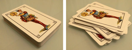
Since all atoms and molecules are attracted to each other by van der Waals (vdW) forces, there are virtually no limitations to how these super-thin materials can be combined into stacks, similar to Lego blocks.
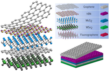
Due to their unique interlayer coupling and optoelectronic properties, these materials are of considerable interest for the next generation nanoelectronics because they make it possible to create high-performance structures tailored to a specific purpose.
Van der Waals heterostructures open a huge potential to create numerous metamaterials and novel devices by stacking together any number of atomically thin layers. This opens up hundreds of combinations that would otherwise be inaccessible with traditional three-dimensional materials, potentially leading to the discovery of new optoelectronic device functionality or unusual material properties.
In addition to the interaction between different 2D atomic layers, the passivated, dangling-bond-free surfaces of 2D crystals can bond to other dimensional materials through van der Waals (vdW) forces. This opens up the possibility of creating mixed-dimensional vdW heterostructures through the hybridization of 2D crystals, such as graphene, with zero-dimensional (0D) quantum dots or nanoparticles, one-dimensional (1D) nanostructures like nanowires or carbon nanotubes, or three-dimensional (3D) bulk materials.
Fabrication
These heterostructures are completely handcrafted and the fabrication procedures presented several drawbacks such as the difficulty to align the crystal lattices (with atomic accuracy) of the different adjacent materials or to avoid trapping ambient adsorbates between the layers, hampering their performance and reproducibility.
However, in 2017, researchers discovered that franckeite, a mineral belonging to the sulfosalts family, shows a natural crystal structure similar to the man-made van der Waals heterostructures – with the huge advantage of an almost perfect alignment between crystal lattices and the absence of tapped residues between layers.
Conventional 2D heterostructures usually are composed of two layers of opposite charge carrier type using inorganic materials. One of the challenges when creating 2D heterostructures is the painstaking stacking of the individual components on top of each other.
Any industrial application will obviously require a scalable approach to the vdW assembly. To this end, significant efforts have been reported to epitaxially grow graphene, 2D hBN and 2D MoS2 on top of each other. However, it is a daunting task to find the right conditions for so-called vdW epitaxy because the weak interlayer interaction generally favours the island growth rather than continuous monolayers.
Another scalable approach is layer by layer deposition from 2D-crystal suspensions by using Langmuir-Blodgett or similar techniques. One can also mix suspensions of different 2D crystals and then make layer-by-layer laminates, relying on self-organizational assembly (flocculation).
Unfortunately, micrometre-sized crystallites in suspensions cannot provide large continuous layers, and this would limit possible applications for such vdW laminates. Currently, they are considered for use as designer ultra-thin dielectrics8, selectively-permeable membranes and composites materials.
The current most practical method for industrial-scale production of van der Waals heterostructures is to grow individual monolayers and few-layers on catalytic substrates, then isolate and stack the 2D sheets on top of each other. This method has already been demonstrated to be scalable. If a particular heterostructure has significant potential applications, it is likely that its production can be scaled up by exploring different available methods.
Read a comprehensive review on van der Waals heterostructures by Andre Geim.
