Metamaterials and Metasurfaces: Engineered Structures Revolutionizing Light and Matter Interactions
Table of Contents
- 1. What are metamaterials and what can they do?
- 2. How do metamaterials work?
- 3. Negative refraction
- 4. What are metasurfaces?
- 5. What do metamaterials allow us to do that couldn't be done before?
- 6. Applications of metamaterials
- 7. Acoustic metamaterials
- 8. Frequently Asked Questions about Metamaterials
Key Takeaways About Metamaterials
- Definition: Metamaterials are engineered structures with properties not found in nature, derived from their microstructure rather than chemical composition
- Core Concept: They manipulate electromagnetic waves (including light) through precisely arranged artificial "atoms" and "molecules" at the micro/nanoscale
- Unique Capability: Can achieve negative refractive index, bending light backwards as it enters the structure
- Metasurfaces: 2D versions of metamaterials that overcome fabrication challenges while maintaining many unique properties
- Applications: Include invisibility cloaking, superlenses that surpass diffraction limits, enhanced solar cells, and acoustic wave manipulation
- Historical Development: Theoretical prediction in mid-20th century, with first practical implementations in early 2000s
- Future Potential: Revolutionary applications in optics, imaging, communications, energy harvesting, and medical technologies
What are metamaterials and what can they do?
The prefix meta (a Greek word meaning ‘beyond’) indicates that the characteristics of the material are beyond what we see in nature. Metamaterials are a novel class of functional materials that are designed around unique micro- and nanoscale patterns or structures, which cause them to interact with light and other forms of energy in ways not found in nature.
Metamaterials are composite materials that are designed and manufactured artificially. Their unique properties are derived from their internal microstructures, rather than from their chemical composition, which is found in natural materials. By manipulating the arrangement of atoms into specific geometries, metamaterials can be engineered to have properties and capabilities that are not possible with natural materials.
Metamaterials are typically built of multiple identical elements fashioned from conventional materials, such as metals or nonconductive materials. Think of a Rubik's cube made of millions of units smaller than the thickness of a human hair.
Steve Cummer, professor of electrical and computer engineering at Duke University, explains the concept of metamaterials using some simple illustrations.
How do metamaterials work?
The essence of metamaterial design lies in creating materials through artificially crafted structural units with specific properties and functions. The structural units, referred to as artificial 'atoms' and 'molecules', can be customized in terms of shape, size, and lattice constant, while interactions between them can be engineered.
Additionally, 'defects' can be strategically placed to further enhance the desired properties. By arranging the nanoscale unit cells in a desired geometry, the refractive index of the metamaterial can be adjusted to positive, near-zero, or negative values.
Negative refraction
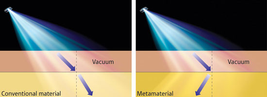
Among the most sought-after properties of metamaterials is the negative index of refraction of light and other radiation. Negative refraction is based on the equations developed in 1861 by Scottish physicist James Maxwell.
All known natural materials have a positive refractive index so that light that crosses from one medium to another gets slightly bent in the direction of propagation. For example, air at standard conditions has the lowest index in nature, hovering just above 1. The index of water is 1.33. That of diamond is about 2.4. The higher a material's refractive index, the more it distorts light from its original path.
In some metamaterials, however, negative refraction occurs such that light and other radiation gets bent backwards as it enters the structure.
The existence of substances with a negative refractive index was predicted as early as the middle of the 20th century. In 1976 Soviet physicist V.G. Veselago published an article that theoretically describes their properties, including an unusual refraction of light. The term metamaterials for such substances was suggested by Roger Walser in 1999.
But only in the early 2000s have researchers figured out how to create materials of any type that can achieve negative refraction. The first samples of metamaterials were made from arrays of thin wires and only worked with microwave radiation.
With such negative refraction materials many applications become possible in electronics manufacturing, lithography, biomedicine, insulating coatings, heat transfer, space applications, and perhaps new approaches to optical computing and energy harvesting.
What are metasurfaces?
The fascinating functionalities of metamaterials typically require multiple stacks of material layers, which not only leads to extensive losses but also brings a lot of challenges in nanofabrication. Many metamaterials consist of complex metallic wires and other structures that require sophisticated fabrication technology and are difficult to assemble.
The unusual optical effects do not necessarily imply the use of the volumetric (3D) metamaterials. You can also manipulate the light with the help of two-dimensional (2D) structures – so-called metasurfaces (or flat optics or meta-optics).
Metasurfaces are thin-films composed of individual elements that have initially been developed to overcome the obstacles that metamaterials are confronted with.
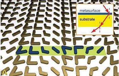
The principle of operation of metasurfaces is based on the phenomenon of diffraction. Any flat periodic array can be viewed as a diffraction lattice, which splits the incident light into a few rays. The number and direction of the rays depends on geometrical parameters: the angle of incidence, wavelength and the period of the lattice.
The structure of the subwavelength unit cell, in turn, determines how the energy of the incident light is distributed between the rays. For a negative refractive index it is necessary that all but one of the diffraction rays are suppressed, then all of the incident light will be directed in the required direction.
So far, most fabricated metasurfaces are passive, meaning that they cannot be tuned post fabrication. In contrast, active metasurfaces allow the dynamic control of its optical properties under external stimuli. They could be useful in applications ranging from free space optical communications to holographic displays, and depth sensing.
What do metamaterials allow us to do that couldn't be done before?
Metamaterials offer the potential to precisely control the path of light in a material. This allows the transformation of traditionally bulky optical systems to extremely small form factors. Metamaterials can also be customized to support novel properties that currently are not accessible with existing optical hardware, leading to entirely new optical systems.
Conventional materials interact with electromagnetic radiation like light or radio waves based on the properties of the material. We are used to how glass bends light or how gold reflects light. In our everyday encounters with these objects, we know what to expect because there’s nothing special about these materials usually.
For instance, you expect gold to be all shiny and yellowish. But when you alter the surface of the gold with nanoscale structures, that changes how the light behaves when it hits the gold surface and that changes how we see it. These nano structures take gold from a conventional material to a metamaterial.
And although nothing about the gold’s chemical properties have changed, we could now be seeing it as blue or red.
You could make the same changes to electromagnetic waves outside the visible spectrum or to audio waves.
These designer materials work by bending the paths of electromagnetic radiation – not only from visible light but also from radio waves to high-energy gamma rays – in new and different ways.
Applications of metamaterials
Optical camouflage and invisibility cloaks
How metamaterials bend the paths of electromagnetic radiation (i.e. refraction) drives their peculiar applications. For example, a metamaterial invisibility cloak would bend the paths of light waves around a cloaked object, accelerating them on their way, and reunite them on the other side. Thus, an onlooker could see what was behind the object, while the object itself would be invisible.
Optical camouflage (such as an invisibility cloaking device) is a technology to make an object seem invisible by causing incident light to avoid the object, flow around the object, and return undisturbed to its original trajectory.
Such sophisticated manipulation of light will probably be realistic thanks to the recent progress in the research on metamaterials. To date several research institutes have carried out the theoretical and experimental study of invisibility camouflage devices, using the extraordinary optical properties of metamaterials and the technique of transformation optics.
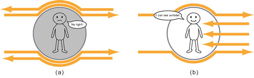
Optical camouflage devices designed using transformation optics have a closed region that incident light from every direction avoids. A person hiding in this region therefore seems invisible to external onlookers.
However, no light can enter the cloaked region, and consequently the person hiding therein cannot be able to see outside. This is quite inconvenient for practical use. A practical camouflage device must have unidirectional transparency such that a person inside cannot be seen from the outside but can see the outside.
Improved solar cells
A metamaterial could be tuned to better match the solar spectrum, allowing for the development of broadband wide-angle metamaterials that could enhance light collection in solar cells. And metamaterials with a wide-angle response can accept light from a broad range of angles. In the case of solar cells, this means more light collection and less reflected or 'wasted' light.
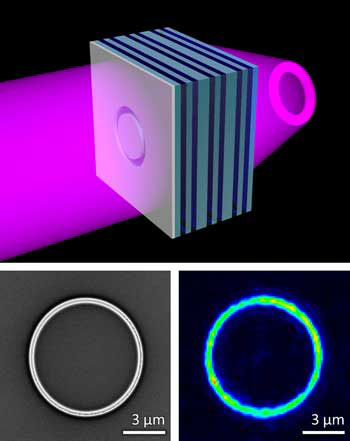
Superlens
One metamaterial application of particular interest is a superlens, a device that might provide light magnification at levels that dwarf any existing technology.
The concept of a 'superlens' has attracted significant research interest in the imaging and photolithography fields since the concept was proposed back in 2000 (see the original paper by Pendry in Physical Review Letters: "Negative Refraction Makes a Perfect Lens").
A superlens allows to view objects much smaller than the roughly 200 nanometers that a regular optical lens with visible light would permit. This theoretical resolution limit (diffraction limit) of conventional optical imaging methodology was the primary factor motivating the development of higher-resolution scanning probe techniques. Though scanning electron microscopes can capture objects that are much smaller, down to the single nanometer range, they are expensive, heavy, and, at the size of a large desk, not very portable.
The superlens concept relies on the generation of surface plasmon polaritons enhancing the evanescent fields to restore the near-field components of the Fourier decomposition of the source object, hence breaking the diffraction limit.
Since superlenses have demonstrated the capability of subdiffraction-limit imaging, they have been envisioned as a promising technology for potential nanophotolithography. Already, superlens lithography is able to demonstrate the required sub-diffraction-limit resolution and high contrast performance required for cost-effective and high throughput nanopatterning mass production (Nano Letters, "High Aspect Subdiffraction-Limit Photolithography via a Silver Superlens").
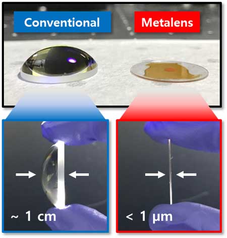
Since these metalenses are ultrathin, flat surfaces, they have attracted tremendous attention because they can overcome limitations of conventional bulky, curved and heavy optical lenses and they are poised to revolutionize everything from microscopy to cameras, sensors, and displays (read more: "Printable nanocomposite overcomes the manufacturing limitations of metalenses").
Acoustic metamaterials
Acoustic metamaterials could be used in many applications. Large versions could be used to direct or focus sound to a particular location and form an audio hotspot. Much smaller versions could be used to focus high intensity ultrasound to destroy tumors deep within the body. Here, a metamaterial layer could be tailor-made to fit the body of a patient and tuned to focus the ultrasound waves where they are needed most.
Researchers have fabricated a metamaterial lens that focuses radio waves with extreme precision. The concave lens exhibits a property called negative refraction, bending electromagnetic waves — in this case, radio waves — in exactly the opposite sense from which a normal concave lens would work.
Concave lenses typically radiate radio waves like spokes from a wheel. In this new metamaterial lens, however, radio waves converge, focusing on a single, precise point – a property impossible to replicate in natural materials.
The device, which weighs less than a pound, may be used to focus radio waves precisely on molecules to create high-resolution images — images that are currently produced using bulky, heavy and expensive lenses. Such a lightweight device could also be mounted on satellites to image stars and other celestial bodies in space where you don’t want to bring up a hefty lens.
Akin to metamaterials that can be used to manipulate wave phenomena such as radar, sound and light, metamaterials are also able to control environmental sounds and structural vibrations, which have similar waveforms.
Finely shaped sound fields are used in medical imaging and therapy as well as in a wide range of consumer products such as audio spotlights and ultrasonic haptics.
Materials with a negative modulus or negative density can trap sounds or vibrations within the structure through local resonances so that they cannot transfer through it; they can also slow down the sound meaning that incoming sound waves can be transformed into any required sound field.
Researchers also have developed a metamaterial that can transport sound in unusually robust ways along its edges and localize it at its corners (Nature Materials, "Observation of higher-order topological acoustic states protected by generalized chiral symmetry"). This unique property may improve technologies that use sound waves, such as sonars and ultrasound devices, making them more resistant to defects.
Frequently Asked Questions about Metamaterials
What exactly are metamaterials?
Metamaterials are artificially engineered structures designed to have properties not found in naturally occurring materials. Their unique properties come from their precisely designed micro- or nanostructures rather than their chemical composition. By arranging conventional materials in specific geometric patterns, metamaterials can manipulate electromagnetic waves, including light, in unprecedented ways.
Who invented metamaterials?
The theoretical foundation for metamaterials was laid in the mid-20th century, with Soviet physicist V.G. Veselago publishing a significant theoretical paper in 1976 describing materials with negative refractive index. The term "metamaterials" was coined by Roger Walser in 1999. However, the first practical metamaterials were created in the early 2000s, with researchers like Sir John Pendry, David Smith, and Willie Padilla making significant contributions to the field.
What is negative refraction and why is it important?
Negative refraction is a phenomenon where light or other electromagnetic waves bend in the opposite direction than they would in conventional materials when crossing from one medium to another. This property, not found in natural materials, is important because it enables revolutionary applications like superlenses that can overcome the diffraction limit of conventional optics, potentially allowing for incredibly detailed imaging beyond what conventional microscopes can achieve.
What's the difference between metamaterials and metasurfaces?
Metamaterials are three-dimensional structures that manipulate electromagnetic waves through their volumetric properties. Metasurfaces, in contrast, are two-dimensional versions of metamaterials—essentially thin films composed of engineered elements. Metasurfaces were developed to overcome fabrication challenges associated with complex 3D metamaterials while still maintaining many of their unique properties. They operate based on diffraction principles and can be easier to manufacture while still allowing manipulation of light and other waves.
Are invisibility cloaks actually possible with metamaterials?
Yes, metamaterials can theoretically create invisibility effects by bending light waves around an object and reuniting them on the other side, making the object effectively invisible to an observer. While full invisibility cloaks like those in science fiction aren't yet reality, researchers have successfully demonstrated metamaterial-based invisibility for specific wavelengths and under controlled conditions. Current research focuses on asymmetric camouflage devices that allow the hidden person to see outside while remaining invisible to external observers from certain directions.
What are acoustic metamaterials?
Acoustic metamaterials are engineered structures designed to control, direct, and manipulate sound waves in ways not possible with conventional materials. Similar to their electromagnetic counterparts, acoustic metamaterials can exhibit properties like negative refraction for sound waves. Applications include focused audio hotspots, high-intensity ultrasound for medical treatments, sound insulation, vibration control, and improved sonars and ultrasound devices that are more resistant to defects.
What are superlenses and how do they work?
Superlenses are devices made from metamaterials that can overcome the diffraction limit of conventional optics, potentially allowing imaging of objects much smaller than 200 nanometers (the typical limit for conventional optical lenses). They work by enhancing evanescent fields through surface plasmon polaritons, restoring near-field components that would normally be lost, and thus capturing details smaller than the wavelength of light used for imaging. This technology has promising applications in nanoscale imaging and photolithography for semiconductor manufacturing.
Are metamaterials currently used in commercial products?
Yes, metamaterials are beginning to appear in commercial applications, though many remain in development. Current commercial uses include specialized antennas, sensors, telecommunications equipment, and some medical imaging devices. Metalenses, which are flat lenses based on metasurface technology, are particularly promising for applications in cameras, displays, and various optical systems due to their compact size and potentially superior performance compared to traditional bulky lenses.
