Van der Waals Revolution: Materials, Heterostructures, and Magnetic Phenomena
Definition: Van der Waals materials encompass a broad category of layered substances, including individual van der Waals materials and their engineered stacks known as van der Waals heterostructures, marked by their unique magnetic, electronic, and optical properties pivotal for advancing nanotechnology and materials science.
Introduction to Van der Waals Materials
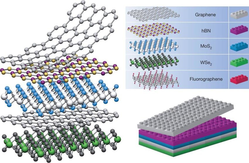
Van der Waals materials consist of layers of atoms or molecules bonded through van der Waals forces, which are weak, distance-dependent interactions between atoms or molecules. Notable examples include graphene, hexagonal boron nitride (hBN), and transition metal dichalcogenides (TMDs). These materials exhibit exceptional electronic, optical, and mechanical properties that are exploitable in various high-tech applications.
Van der Waals Heterostructures
Van der Waals heterostructures are engineered by stacking different van der Waals materials in a controlled sequence, allowing the creation of new materials with tailored properties. This technique enables the combination of disparate materials, such as semiconductors and insulators, to fabricate devices with optimized performance for electronics, photonics, and energy storage applications.
Magnetic Van der Waals Materials
A subset of van der Waals materials exhibits magnetic properties, which are of particular interest for spintronics, a field that utilizes the spin of electrons in addition to their charge for information processing. Magnetic van der Waals materials can exhibit ferromagnetism, antiferromagnetism, or other magnetic orders at the nanoscale, enabling the development of ultra-thin magnetic devices.
Key Features and Applications
The layered structure of van der Waals materials facilitates electron mobility, making them ideal for electronic and optoelectronic devices. Heterostructures expand these capabilities, offering engineered band gaps, enhanced light-matter interactions, and tailored thermal properties. Magnetic van der Waals materials add functionalities for data storage and quantum computing, highlighting the versatility of these materials in advancing technology.
Challenges and Future Directions
Despite their potential, challenges remain in synthesizing high-quality van der Waals materials and heterostructures, particularly in controlling layer thickness, composition, and stacking order. Advances in fabrication techniques and a deeper understanding of their properties are crucial for their integration into practical applications. The exploration of magnetic van der Waals materials continues to open new avenues in magnetism and spintronics, promising further innovations in technology.
Environmental and Sustainable Applications
Van der Waals materials and heterostructures are also being explored for environmental and sustainable applications, offering promising solutions in clean energy, pollution control, and beyond. Their ability to be engineered at the atomic level for specific functions presents opportunities for creating more efficient and environmentally friendly technologies.
Impact on Industry and Research
The ongoing research and development of van der Waals materials, including their magnetic variants and heterostructures, are poised to revolutionize industries ranging from electronics and energy to biomedicine. Their unique properties and potential for innovation continue to draw significant interest, shaping the future of materials science and technology.
Further Reading
Nature Reviews Physics, Van der Waals heterostructures and devices
International Journal of Extreme Manufacturing, Fabrication and applications of van der Waals heterostructures
