| Jan 07, 2019 |
Graphene and other 2D materials for advanced solar cells |
| (Nanowerk Spotlight) Inorganic crystalline silicon solar cells account for more than 90% of the market despite a recent surge in research efforts to develop new architectures and materials such as organics and perovskites. |
| The reason why most commercial solar cells are using crystalline silicon as the absorber layer include long-term stability, the abundance of silicone, relatively low manufacturing costs, ability for doping by other elements, and native oxide passivation layer. |
| However, the indirect band gap nature of crystalline silicon makes it a poor light emitter, limiting its solar conversion efficiency. For instance, compared to the extraordinary high light absorption coefficient of perovskites, silicon requires 1,000 times more material to absorb the same amount of sunlight. |
| In order to reduce the cost per watt and improve watt per gram utilization of future generations of solar cells, reducing the active absorber thickness is a key design requirement. This is where novel two-dimensional (2D) materials like graphene come into play because they could lead to thinner, lightweight and flexible solar cells. |
| Experimental designs for several graphene-based solar cells have been reported so far, with graphene serving as different parts of the cell. |
| Due to their excellent electron-transport properties and extremely high carrier mobility, not only graphene but also other direct bandgap monolayer materials such as transition-metal dichalcogenides (TMDCs) and black phosphorus show great potential to be used for low-cost, flexible, and highly efficient photovoltaic devices. |
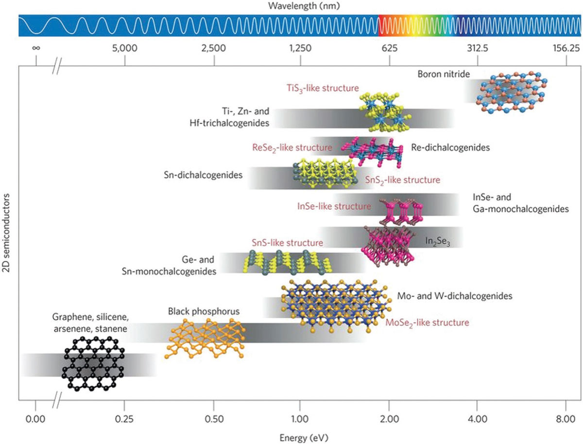 |
| Comparison of the bandgap values for different 2D semiconductor materials families. The crystal structure is also displayed to highlight the similarities and differences between the different families. The gray horizontal bars indicate the range of bandgap values that can be spanned by changing the number of layers, straining, or alloying. This broad bandgap range spanned by all these 2D semiconductors can be exploited in a wide variety of photonics and optoelectronics applications, such as thermal imaging, fiber optics communication, photovoltaics, displays, and light-emitting diodes. (© Springer Nature) (click on image to enlarge) |
| A recent review in Advanced Materials ("The Role of Graphene and Other 2D Materials in Solar Photovoltaics") provides a comprehensive overview on the current state-of-the-art of 2D-materials-based solar photovoltaics. It describes the recent progress made with graphene, graphene-based materials, and other 2D materials for solar photovoltaics, including silicon-based solar cells, and organic and perovskite solar cells. |
Graphene-based solar cells |
| In the first part of their review, the authors present the role of doped and undoped graphene as an ultrathin, transparent conducting electrode, and as a Schottky barrier junction layer (hole collector) for silicon-based solar cells. This section also discusses graphene (undoped/doped) as a charge-transport layer/transparent electrode for organic/perovskite solar cells. |
| In a solar cell, the electric field formed due to the potential energy barrier between two dissimilar materials at the interface is capable of separating the electrons and holes generated by absorption of light within the materials. Based on the type of materials at the interface, there are three types of junctions, which are homojunction, heterojunction (formed between two different semiconductors having different energy bandgaps), and Schottky junction (a metal???semiconductor junction where band bending occurs). |
| While graphene allows better transmission of light into the semiconductor, it also forms a Schottky barrier junction with silicon for effective separation of the electron???hole pairs and collection of the charge carriers. The authors discuss in detail the role of graphene as transparent conducting electrodes and as junction layers (hole collectors) in graphene???Si solar cells. |
| ITO, which has a key role as a transparent conductive electrode for organic-based and perovskite-based solar cells, suffers from some disadvantages. In these organic solar cells, graphene – due to its high conductivity, desired work function, and optimum surface morphology – can act as a potential substitute for ITO, while offering similar performance with respect to transparency, conductivity, flexibility, with higher material availability and lower processing costs. |
| The review in great detail covers the role of graphene-based materials for electrodes, charge-transport layers, and tenary materials for organic solar cells as well as charge-transport layers and stabilizing material for perovskite solar cells. |
 |
| Schematic of the different types of 2D-material-based solar cells. (Reprinted with permission by Wiley-VCH Verlag) |
The role of 2D materials beyond graphene for solar-cell applications |
| Theoretically, a single TMDC monolayer with sub-nanometer thickness has the capability to absorb as much sunlight as 50 nm of Si or 15 nm gallium arsenide (GaAs) and, therefore, can generate electric currents as high as 4.5 mA cm-2. |
| The authors discuss and calculate the potential performance of TDMCs for silicon-based solar cells, organic solar cells, and perovskite solar cells. |
The concept of superthin 2D/2D heterojunction solar cells |
| The authors point out that "the idea of an all-2D solar cell may not seem very effective from a photovoltaic standpoint, since conventionally used active materials are a lot thicker, thus absorbing more sunlight. However, interestingly, such solar cells have the potential to surpass the performance of conventional photovoltaics based on Si and GaAs. TMDCs have a bandgap in the visible to near-infrared part of the spectrum, which makes them ideal for solar-cell applications." |
| "Furthermore, being direct-bandgap semiconductors at monolayer thickness, they allow high radiative efficiency. This, when coupled to their significantly higher absorption coefficient per unit thickness (greater than Si, GaAs, and perovskites) makes them suitable for highly absorbing ultrathin photovoltaic devices. The strong absorption in atomically thin layers with sharp, clean interfaces allows the highest watt-per-gram utilization of the active material." |
Next-generation 2D photovoltaics |
| In the final section of the review, next-generation concepts such as tandem and hot-carrier solar cells based on 2D materials, and on-chip integrated design of energy harvesting and storage devices are discussed, leading to an ideal solar cell where the entire energy of any absorbed photon is harvested. |
| Concluding their review, the authors present a brief outlook for meeting the challenges and requirements for next-generation 2D photovoltaics at low cost and high production rate. "We feel that graphene has already demonstrated tremendous research and industrial potential and can be imbibed into the standard technology roadmap of photovoltaics. One concern to this end is that it has to compete with established processes and supply chains for existing materials like silicon and indium tin oxide. However, we feel that materials with immense potential should always synergistically supplement and compliment, rather than compete, with each other." |
 By
Michael
Berger
– Michael is author of four books by the Royal Society of Chemistry:
Nano-Society: Pushing the Boundaries of Technology (2009),
Nanotechnology: The Future is Tiny (2016),
Nanoengineering: The Skills and Tools Making Technology Invisible (2019), and
Waste not! How Nanotechnologies Can Increase Efficiencies Throughout Society (2025)
Copyright ©
Nanowerk LLC
By
Michael
Berger
– Michael is author of four books by the Royal Society of Chemistry:
Nano-Society: Pushing the Boundaries of Technology (2009),
Nanotechnology: The Future is Tiny (2016),
Nanoengineering: The Skills and Tools Making Technology Invisible (2019), and
Waste not! How Nanotechnologies Can Increase Efficiencies Throughout Society (2025)
Copyright ©
Nanowerk LLC
|

Become a Spotlight guest author! Join our large and growing group of guest contributors. Have you just published a scientific paper or have other exciting developments to share with the nanotechnology community? Here is how to publish on nanowerk.com. |
