What are Nanomaterials?
Content
Definition of Nanomaterials
Nanomaterials are materials with at least one external dimension that measures 100 nanometers (nm) or less or with internal structures measuring 100 nm or less. The nanomaterials that have the same composition as known materials in bulk form may have different physico-chemical properties.
Materials reduced to the nanoscale can suddenly show very different properties compared to what they show on a macroscale. For instance, opaque substances become transparent (copper); inert materials become catalysts (platinum); stable materials turn combustible (aluminum); solids turn into liquids at room temperature (gold); insulators become conductors (silicon).
Nanomaterials are not simply another step in the miniaturization of materials or particles. They often require very different production approaches. There are several processes to create various sizes of nanomaterials, classified as ‘top-down’ and ‘bottom-up’.
Nanomaterials can be constructed by top down techniques, producing very small structures from larger pieces of material, for example by etching to create circuits on the surface of a silicon microchip.
They may also be constructed by bottom up techniques, atom by atom or molecule by molecule. One way of doing this is self-assembly, in which the atoms or molecules arrange themselves into a structure due to their natural properties. Crystals grown for the semiconductor industry provide an example of self assembly, as does chemical synthesis of large molecules.
Although this 'positional assembly' offers greater control over construction, it is currently very laborious and not suitable for industrial applications.
Check out our detailed article on how nanoparticles are made.
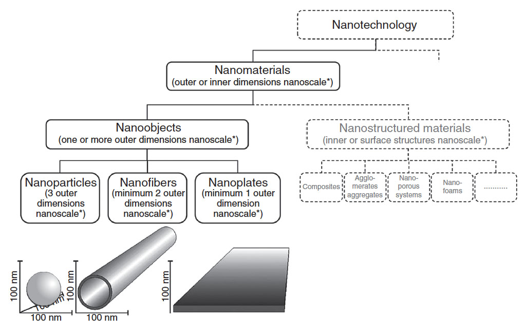
The ISO definition of nano-objects. Included as nano-objects are nanoparticles (nanoscale in all the three dimensions), nanofibers (nanoscale in two dimensions), and nanosheets or nanolayers (nanoscale only in one dimension) that include graphene and MXenes. (© John Wiley & Sons) (click to enlarge)
Applications of Nanomaterials
If you check our links in the right column of this page you can explore lots of areas where nanotechnology and nanomaterials are currently used. So we don't have to repeat this here. Suffice it to say that nanotechnology already has become ubiquitous in daily life through commodity products and growth rates are strong.
The chart below shows how products involving nanomaterials and nanotechnology are distributed across industries:
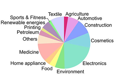
Global nanotechnology market by industry branches. (Source: doi:10.1021/acsnano.1c03992)
Analyzing nanotechnology revenues by sector reveals that materials and manufacturing contributed the most to total nanotechnology revenue. Such a trend is expected considering that the first stage of development in creating any general purpose technology includes foundational interdisciplinary research, which in case of nanotechnology translates into the discovery of material properties and synthesis of nanoscale components. However, in the upcoming years we can expect this trend to shift more toward application sectors as nanodevices are amalgamated with existing technologies.
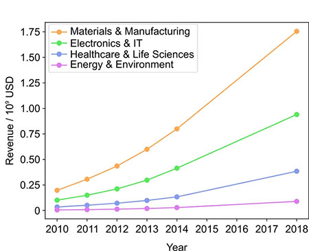
Overview of revenues generated by nanotechnology (USD billions). Gross revenue generated from nanotechnology products, as grouped by industry sector and in the 2010–2018 period. (Source: doi:10.1021/acsnano.1c03992)
Definition of Nanomaterials
If 50% or more of the constituent particles of a material in the number size distribution have one or more external dimensions in the size range 1 nm to 100 nm, then the material is a nanomaterial. It should be noted that a fraction of 50% with one or more external dimensions between 1 nm and 100 nm in a number size distribution is always less than 50% in any other commonly-used size distribution metric, such as surface area, volume, mass or scattered light intensity. In fact it can be a tiny fraction of the total mass of the material.
Even if a product contains nanomaterials, or when it releases nanomaterials during use or aging, the product itself is not a nanomaterial, unless it is a particulate material itself that meets the criteria of particle size and fraction.
The volume specific surface area (VSSA) can be used under specific conditions to indicate that a material is a nanomaterial. VSSA is equal to the sum of the surface areas of all particles divided by the sum of the volumes of all particles. VSSA > 60 m2/cm3 is likely to be a reliable indicator that a material is a nanomaterial unless the particles are porous or have rough surfaces, but many nanomaterials (according to the principal size-based criterion) will have a VSSA of less than 60 m2/cm3. The VSSA > 60 m2/cm3 criterion can therefore only be used to show that a material is a nanomaterial, not vice versa. The VSSA of a sample can be calculated if the particle size distribution and the particle shape(s) are known in detail. The reverse (calculating the size distribution from the VSSA value) is unfeasible.
Dimensions of Nanomaterials
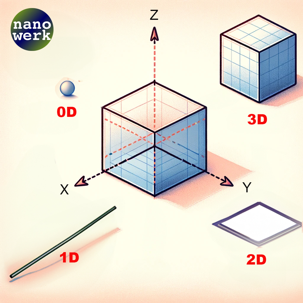
Nanomaterials are primarily categorized based on the dimensional characteristics they display. These dimensions are classified as zero-dimensional (0D), one-dimensional (1D), two-dimensional (2D), and three-dimensional (3D) nanomaterials, all of which fall within the nanoscale range.
Classification of nanoscale dimensions. (© Nanowerk)
Quantum dots and small nanoparticles are often referred to as "zero-dimensional" (0D) structures, despite having three physical dimensions. This might sound confusing at first, but it’s because we’re talking about their quantum mechanical properties rather than their geometric shape. Let's unpack this a bit:
Quantum Confinement in All Three Dimensions: In quantum dots or small nanoparticles, electrons experience quantum confinement in all three dimensions, much like being restricted in an extremely tiny room. This confinement is effective when the size of the particle is comparable to or smaller than what is called the “exciton Bohr radius” of the material, which is typically a few nanometers This confinement limits the electrons to specific energy levels, their “discret energy levels.” Think of it as a game of musical chairs at the quantum scale: the electrons, like players in the game, can only occupy certain 'seats' or energy states.
The number of these available 'seats' is determined by several factors:
As a result of these combined factors, electrons in quantum dots have a limited set of energy levels they can occupy, akin to having a set number of chairs in the room. This is a stark contrast to larger, bulk materials where electrons have a more continuous range of energy levels available.
Exciton Bohr Radius: The exciton Bohr radius is a key factor in determining the size limit. It is like a measuring stick that tells us how small we need to make our nanoparticle to see its cool quantum effects. It varies between materials but is generally in the range of a few nanometers. When the size of the nanoparticle is smaller than or similar to this radius, quantum confinement effects are significant, and the particle behaves as a 0D system.
Size and Quantum Effects: The size of quantum dots is typically 2-10 nanometers. At this scale, the quirky rules of quantum mechanics start to dominate, making these particles behave very differently from larger pieces of the same material.
Comparison with Higher Dimensions: In our room analogy above, think of 1D and 2D materials, like nanowires and thin films, as narrow hallways and wide floors. Electrons can move freely along these hallways or floors but can’t jump out of them. This partial freedom leads to different behaviors compared to the completely confined quantum dots or nanoparticles.
Transition to 3D Behavior: As the size of the nanoparticle gets bigger, beyond the exciton Bohr radius, it starts behaving more like a regular, bulk material. The electrons begin to move more freely, akin to how water starts to flow when a dam is opened, leading to a more continuous range of energy levels. This marks the transition towards 3D behavior.
Material-Dependent Threshold: The exact size at which this transition occurs depends on the material of the nanoparticle. Different materials have different exciton Bohr radii and therefore different thresholds for the transition from quantum-confined (0D) behavior to bulk-like (3D) behavior.
Gradual Transition: It's important to note that the transition from 0D to 3D behavior is not abrupt but gradual. As the nanoparticle grows, its energy levels slowly spread out, moving from distinct steps on a ladder to more of a ramp. Accordingly, a material's physical properties change as the energy levels evolve from discrete to continuous.
To sum up the dimensionality issue in nanomaterials, each class—zero-dimensional (0D), one-dimensional (1D), two-dimensional (2D), and three-dimensional (3D)—displays unique properties due to the extent of quantum confinement. In 0D materials, electrons are confined in all dimensions, leading to atom-like behaviors. In 1D materials, such as nanowires, confinement occurs in two dimensions, allowing electron movement in one direction. 2D materials, like graphene, confine electrons in a plane, resulting in unique electronic and physical properties. Finally, 3D materials, where quantum effects diminish, resemble bulk materials but with enhanced surface properties due to their nanoscale dimensions. Each dimensionality offers distinct physical, chemical, and electronic characteristics, making them suitable for various applications in science and technology. The transition from 0D to 3D is not abrupt but gradual, with properties evolving as the dimensionality increases, leading to a diverse spectrum of behaviors and potential applications in the realm of nanotechnology.
In zero-dimensional (0D) nanomaterials, all dimensions are confined to the nanoscale, typically not exceeding 100 nm. This category primarily includes quantum dots and nanoparticles, where electrons are quantum confined in all three spatial dimensions, leading to unique optical and electronic properties.
One-dimensional (1D) nanomaterials, such as nanotubes, nanorods, and nanowires, have one dimension that extends beyond the nanoscale, allowing electron movement along their length. This unique structure endows them with distinct mechanical, electrical, and thermal properties.
Two-dimensional (2D) nanomaterials are characterized by having two dimensions beyond the nanoscale. These materials, including graphene, nanofilms, and nanocoatings, are essentially ultra-thin layers where electrons are free to move along the plane but are confined in the perpendicular direction. This results in exceptional surface area, electrical conductivity, and strength.
Three-dimensional (3D) nanomaterials are those in which none of the dimensions are confined to the nanoscale. This diverse class includes bulk powders, dispersions of nanoparticles, aggregates of nanowires and nanotubes, and layered structures. In these materials, the unique properties of nanoparticles are combined with bulk material behaviors, leading to a wide range of applications and functionalities.
The chart below shows the distribution of nanomaterial dimensionality in commercialized products. Data show that 3D nanomaterials are the most abundant (85% of all materials), in particular nanoparticles, which are currently present in 78% of all nanoproducts.
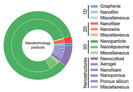
Distribution of nanomaterial dimensionality in commercialized products. (Source: doi:10.1021/acsnano.1c03992)
Properties of Nanomaterials
Below we outline some examples of nanomaterials that are aimed at understanding their properties. As we will see, the behavior of some nanomaterials is well understood, whereas others present greater challenges.
Nanoscale in One Dimension
Thin films, layers and surfaces
One-dimensional nanomaterials, such as thin films and engineered surfaces, have been developed and used for decades in fields such as electronic device manufacture, chemistry and engineering.
In the silicon integrated-circuit industry, for example, many devices rely on thin films for their operation, and control of film thicknesses approaching the atomic level is routine.
Monolayers (layers that are one atom or molecule deep) are also routinely made and used in chemistry. The most important example of this new class of materials is graphene.
The formation and properties of these layers are reasonably well understood from the atomic level upwards, even in quite complex layers (such as lubricants) and nanocoatings. Advances are being made in the control of the composition and smoothness of surfaces, and the growth of films.
Engineered surfaces with tailored properties such as large surface area or specific reactivity are used routinely in a range of applications such as in fuel cells and catalysts. The large surface area provided by nanoparticles, together with their ability to self assemble on a support surface, could be of use in all of these applications.
Although they represent incremental developments, surfaces with enhanced properties should find applications throughout the chemicals and energy sectors.
The benefits could surpass the obvious economic and resource savings achieved by higher activity and greater selectivity in reactors and separation processes, to enabling small-scale distributed processing (making chemicals as close as possible to the point of use). There is already a move in the chemical industry towards this.
Another use could be the small-scale, on-site production of high value chemicals such as pharmaceuticals.
Graphene and other single- and few-layer materials
Graphene is an atomic-scale honeycomb lattice made of carbon atoms. Graphene is undoubtedly emerging as one of the most promising nanomaterials because of its unique combination of superb properties, which opens a way for its exploitation in a wide spectrum of applications ranging from electronics to optics, sensors, and biodevices.
For instance, graphene-based nanomaterials have many promising applications in energy-related areas. Just some recent examples: Graphene improves both energy capacity and charge rate in rechargeable batteries; activated graphene makes superior supercapacitors for energy storage; graphene electrodes may lead to a promising approach for making solar cells that are inexpensive, lightweight and flexible; and multifunctional graphene mats are promising substrates for catalytic systems (read more:graphene nanotechnology in energy).
We also compiled a primer on graphene applications and uses. And don't forget to read our much more extensive explainer What is graphene?
The fascination with atomic-layer materials that has started with graphene has spurred researchers to look for other 2D structures like for instance metal carbides and nitrides.
One particularly interesting analogue to graphene would be 2D silicon – silicene – because it could be synthesized and processed using mature semiconductor techniques, and more easily integrated into existing electronics than graphene is currently.
Another material of interest is 2D boron, an element with worlds of unexplored potential. And yet another new two-dimensional material – made up of layers of crystal known as molybdenum oxides – has unique properties that encourage the free flow of electrons at ultra-high speeds.
Nanoscale in Two Dimension
Two dimensional nanomaterials such as tubes and wires have generated considerable interest among the scientific community in recent years. In particular, their novel electrical and mechanical properties are the subject of intense research.
Carbon nanotubes
Carbon nanotubes (CNTs) were first observed by Sumio Iijima in 1991. CNTs are extended tubes of rolled graphene sheets. There are two types of CNT: single-walled (one tube) or multi-walled (several concentric tubes). Both of these are typically a few nanometers in diameter and several micrometers to centimeters long.
CNTs have assumed an important role in the context of nanomaterials, because of their novel chemical and physical properties. They are mechanically very strong (their Young’s modulus is over 1 terapascal, making CNTs as stiff as diamond), flexible (about their axis), and can conduct electricity extremely well (the helicity of the graphene sheet determines whether the CNT is a semiconductor or metallic). All of these remarkable properties give CNTs a range of potential applications: for example, in reinforced composites, sensors, nanoelectronics and display devices.
CNTs are now available commercially in limited quantities. They can be grown by several techniques. However, the selective and uniform production of CNTs with specific dimensions and physical properties is yet to be achieved. The potential similarity in size and shape between CNTs and asbestos fibers has led to concerns about their safety.
Inorganic nanotubes
Inorganic nanotubes and inorganic fullerene-like materials based on layered compounds such as molybdenum disulphide were discovered shortly after CNTs. They have excellent tribological (lubricating) properties, resistance to shockwave impact, catalytic reactivity, and high capacity for hydrogen and lithium storage, which suggest a range of promising applications. Oxide-based nanotubes (such as titanium dioxide) are being explored for their applications in catalysis, photo-catalysis and energy storage.
Nanowires
Nanowires are ultrafine wires or linear arrays of dots, formed by self-assembly. They can be made from a wide range of materials. Semiconductor nanowires made of silicon, gallium nitride and indium phosphide have demonstrated remarkable optical, electronic and magnetic characteristics (for example, silica nanowires can bend light around very tight corners).
Nanowires have potential applications in high-density data storage, either as magnetic read heads or as patterned storage media, and electronic and opto-electronic nanodevices, for metallic interconnects of quantum devices and nanodevices.
The preparation of these nanowires relies on sophisticated growth techniques, which include self-assembly processes, where atoms arrange themselves naturally on stepped surfaces, chemical vapor deposition (CVD) onto patterned substrates, electroplating or molecular beam epitaxy (MBE). The ‘molecular beams’ are typically from thermally evaporated elemental sources.
Biopolymers
The variability and site recognition of biopolymers, such as DNA molecules, offer a wide range of opportunities for the self-organization of wire nanostructures into much more complex patterns. The DNA backbones may then, for example, be coated in metal. They also offer opportunities to link nano- and biotechnology in, for example, biocompatible sensors and small, simple motors.
Such self-assembly of organic backbone nanostructures is often controlled by weak interactions, such as hydrogen bonds, hydrophobic, or van der Waals interactions (generally in aqueous environments) and hence requires quite different synthesis strategies to CNTs, for example.
The combination of one-dimensional nanostructures consisting of biopolymers and inorganic compounds opens up a number of scientific and technological opportunities.
Nanoscale in Three Dimensions
Nanoparticles
Nanoparticles are often defined as particles of less than 100nm in diameter. We classify nanoparticles to be particles less than 100nm in diameter that exhibit new or enhanced size-dependent properties compared with larger particles of the same material.
Nanoparticles exist widely in the natural world: for example as the products of photochemical and volcanic activity, and created by plants and algae. They have also been created for thousands of years as products of combustion and food cooking, and more recently from vehicle exhausts. Deliberately manufactured nanoparticles, such as metal oxides, are by comparison in the minority.
Nanoparticles are of interest because of the new properties (such as chemical reactivity and optical behavior) that they exhibit compared with larger particles of the same materials.
For example, titanium dioxide and zinc oxide become transparent at the nanoscale, however are able to absorb and reflect UV light, and have found application in sunscreens.
Nanoparticles have a range of potential applications: in the short-term in new cosmetics, textiles and paints; in the longer term, in methods of targeted drug delivery where they could be to used deliver drugs to a specific site in the body.
Nanoparticles can also be arranged into layers on surfaces, providing a large surface area and hence enhanced activity, relevant to a range of potential applications such as catalysts.
Manufactured nanoparticles are typically not products in their own right, but generally serve as raw materials, ingredients or additives in existing products.
Nanoparticles are currently in a number of consumer products such as cosmetics and their enhanced or novel properties may have implications for their toxicity.
For most applications, nanoparticles will be fixed (for example, attached to a surface or within in a composite) although in others they will be free or suspended in fluid. Whether they are fixed or free will have a significant affect on their potential health, safety and environmental impacts.
Fullerenes (carbon 60)
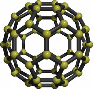
The C60 "buckyball" fullerene
In the mid-1980s a new class of carbon material was discovered called carbon 60 (C60). Harry Kroto and Richard Smalley, the experimental chemists who discovered C60 named it "buckminsterfullerene", in recognition of the architect Buckminster Fuller, who was well-known for building geodesic domes, and the term fullerenes was then given to any closed carbon cage. C60 are spherical molecules about 1nm in diameter, comprising 60 carbon atoms arranged as 20 hexagons and 12 pentagons: the configuration of a football.
In 1990, a technique to produce larger quantities of C60 was developed by resistively heating graphite rods in a helium atmosphere.
Several applications are envisaged for fullerenes, such as miniature ‘ball bearings’ to lubricate surfaces, drug delivery vehicles and in electronic circuits.
Dendrimers
Dendrimers are spherical polymeric molecules, formed through a nanoscale hierarchical self-assembly process. There are many types of dendrimer; the smallest is several nanometers in size. Dendrimers are used in conventional applications such as coatings and inks, but they also have a range of interesting properties which could lead to useful applications.
For example, dendrimers can act as nanoscale carrier molecules and as such could be used in drug delivery. Environmental clean-up could be assisted by dendrimers as they can trap metal ions, which could then be filtered out of water with ultra-filtration techniques.
Quantum dots
Nanoparticles of semiconductors (quantum dots) were theorized in the 1970s and initially created in the early 1980s. If semiconductor particles are made small enough, quantum effects come into play, which limit the energies at which electrons and holes (the absence of an electron) can exist in the particles. As energy is related to wavelength (or color), this means that the optical properties of the particle can be finely tuned depending on its size. Thus, particles can be made to emit or absorb specific wavelengths (colors) of light, merely by controlling their size.
Recently, quantum dots have found applications in composites, solar cells (Grätzel cells) and fluorescent biological labels (for example to trace a biological molecule) which use both the small particle size and tuneable energy levels.
Recent advances in chemistry have resulted in the preparation of monolayer-protected, high-quality, monodispersed, crystalline quantum dots as small as 2nm in diameter, which can be conveniently treated and processed as a typical chemical reagent.
The Key Differences Between Nanomaterials and Bulk Materials
Two principal factors cause the properties of nanomaterials to differ significantly from other materials: increased relative surface area, and quantum effects. These factors can change or enhance properties such as reactivity, strength and electrical characteristics.
As a particle decreases in size, a greater proportion of atoms are found at the surface compared to those inside. For example, a particle of size 30 nm has 5% of its atoms on its surface, at 10 nm 20% of its atoms, and at 3 nm 50% of its atoms.
Thus nanoparticles have a much greater surface area per unit mass compared with larger particles. As growth and catalytic chemical reactions occur at surfaces, this means that a given mass of material in nanoparticulate form will be much more reactive than the same mass of material made up of larger particles.

To understand the effect of particle size on surface area, consider an American Silver Eagle coin. This silver dollar contains 31 grams of coin silver and has a total surface area of approximately 3000 square millimeters. If the same amount of coin silver were divided into tiny particles – say 10 nanometer in diameter – the total surface area of those particles would be 7000 square meters (which is equal to the size of a soccer field – or larger than the floor space of the White House, which is 5100 square meters). In other words: when the amount of coin silver contained in a silver dollar is rendered into 10 nm particles, the surface area of those particles is over 2 million times greater than the surface area of the silver dollar!
Frequently Asked Questions (FAQs) About Nanomaterials
What are nanomaterials?
Nanomaterials are materials that have at least one dimension (height, width, or length) that measures between 1 and 100 nanometers (nm). At this scale, materials can exhibit unique properties that are different from those seen at the micro or macro scale. This can include changes in physical, chemical, or biological properties. Nanomaterials can be composed of various substances, including metals, semiconductors, or organic compounds.
What are the types of nanomaterials?
Nanomaterials can be categorized into four basic types: nanoplates (one dimension under 100 nm), nanorods (two dimensions under 100 nm), nanoparticles (three dimensions under 100 nm), and nanoporous materials. They can also be grouped based on their composition, such as carbon-based, metal-based, dendrimers, composites, and unique substances like quantum dots or liposomes.
How are nanomaterials made?
Nanomaterials can be produced through a variety of methods. Top-down methods involve the reduction of larger materials to the nanoscale, often through physical processes like milling. Bottom-up methods involve the assembly of nanomaterials from atomic or molecular components through processes such as chemical vapor deposition, sol-gel synthesis, or self-assembly.
What properties do nanomaterials have?
Nanomaterials can exhibit a wide range of unique properties depending on their size, shape, and composition. These can include increased strength, light weight, increased control over light spectrum, enhanced magnetic properties, increased reactivity, and unique quantum effects. These properties make nanomaterials useful in a variety of applications.
What are some applications of nanomaterials?
Nanomaterials have diverse applications across many fields. In medicine, they are used in drug delivery systems, imaging, and therapies. In electronics, they're used in the manufacture of transistors, sensors, and other components. Nanomaterials also have uses in energy production and storage, such as in solar panels and batteries. They can be found in consumer products like cosmetics and sunscreens, and in materials science for the creation of stronger, lighter materials.
What are the safety concerns associated with nanomaterials?
Due to their small size and high reactivity, nanomaterials can interact with biological systems in unexpected ways, potentially leading to toxicity. Some nanomaterials can accumulate in the body or environment and their long-term effects are not fully understood. Therefore, there is a need for careful study and regulation of nanomaterials to ensure their safe use.
What is the future of nanomaterials?
The field of nanomaterials is rapidly evolving and holds great promise for the future. Advances in nanotechnology will likely lead to the development of new nanomaterials with tailored properties for specific applications. These could revolutionize fields such as medicine, electronics, energy, and materials science, among others. However, the safe and responsible development and use of nanomaterials will be crucial to their success.
