| Posted: Feb 21, 2008 |
'Cool' graphene might be ideal for thermal management in nanoelectronics |
| (Nanowerk Spotlight) There has been quite a buzz about graphene, a single atomic layer thick, plane of carbon atoms arranged in a honeycomb lattice. Discovered only in 2004, graphene exhibits many exotic properties and currently is considered the most exciting new material system among nanotechnology researchers. This rising star in material science exhibits remarkable electronic properties that qualify it for applications in future optoelectronic devices. |
| In a first experimental study of the thermal conductivity of single-layer graphene, researchers found that on top of many unique electronic properties, graphene also is an extraordinary good heat conductor. Measurements revealed that graphene's near room temperature thermal conductivity, which is in the range from 3500–5300 W/mK, is much higher than that of diamond, the best bulk crystal heat conductor. |
| It appears that the thermal conductivity of graphene is larger than conventionally accepted experimental values reported for individual suspended carbon nanotubes (CNTs) and corresponds to the upper bound of the highest values reported for single-wall CNT bundles. The superb thermal conduction property of graphene is beneficial for its proposed electronic applications and establishes graphene as an excellent material for thermal management also in optoelectronics, photonics and bioengineering. |
| "Our measurement of the thermal conductivity of graphene is the very first one" Dr. Alexander A. Balandin tells Nanowerk. "It required a development of completely new experimental technique and data extraction methodology. The measurements were performed for long graphene flakes suspended across a trench in Si/SiO2 substrate and connected to graphitic heat sinks. Previously, only simple theoretical estimates for the thermal conductivity of graphene were known." |
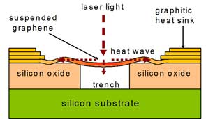 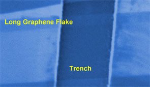 |
| Left: Schematic of the experiment showing the excitation laser light focused on a graphene layer suspended across a trench. The focused laser light creates a local hot spot and generates a heat wave inside SLG propagating toward heat sinks. Right: Scanning electron microscopy image of the suspended single- and few-layer graphene across a trench in Si/SiO2 substrate. (Images: Dr. A.A. Balandin, Ms. S. Ghosh and Dr. C.N. Lau, UC Riverside) |
| Balandin is a professor in the Department of Electrical Engineering at the University of California - Riverside (UCR) and director of the Nano-Device Laboratory. Dr. Chun Ning Lau, whose group contributed and co-authored the research, is an assistant professor in the Department of Physics and Astronomy at UCR. The findings of their interdisciplinary research team were published in the February 20, 2008 online edition of Nano Letters ("Superior Thermal Conductivity of Single-Layer Graphene"). |
| Balandin explains that the main practical motivation for his group's work was the search for a material with an extremely high thermal conductivity, which can be integrated with electronic silicon technology. |
| "These newly discovered excellent heat-conducting properties, combined with its single atom thickness and flat geometry, make graphene an excellent candidate for heat removal and thermal management of future nanoelectronic circuits" says Balandin. "It might be easier to integrate plane graphene layers rather than carbon nanotubes with electronic circuits. As the electronic industry moves towards nanometer designs, one of the most important challenges is the growing chip power consumption. For this reason the thermal management in electronic circuits is becoming an integral part of the design, test and manufacturing" (see our previous Spotlight "Nanotechnology to the rescue of overheating computer chips"). |
| CNTs are known to have very high thermal conductivity with the experimentally determined room temperature value of around 3000 W/mK for an individual multi-walled CNT and about 3500 W/mK for an individual single-walled CNT. These values exceed those of the best bulk crystalline thermal conductor, diamond, which has the thermal conductivity in the range of 1000–2200 W/mK. |
| In spite of the fundamental science and practical importance of the knowledge about the thermal conductivity of graphene, no experimental data has been reported to date. |
| Balandin explains this with the fact that the conventional techniques for measuring the thermal conductivity such as thermal bridge, 3ω method or 'laser-flash', are not well suited for single-layer graphene. "The 3ω method is good for measuring the cross-plane thermal conductivity and requires a substantial temperature drop over the thickness of the examined film" he says. "Graphene with the thickness of one atomic layer and expected high thermal conductivity cannot satisfy such a requirement. The direct thermal-bridge measurements of graphene are possible in principle but very challenging technologically." |
| The UCR team undertook an unconventional approach for the noncontact measurement of the thermal conductivity of graphene by using the confocal micro-Raman spectroscopy. |
| "Several factors, specific for graphene, made it possible" says Balandin. "Graphene has clear signatures in Raman spectra. We have also recently discovered that the G peak in graphene spectra manifest a strong temperature dependence. The G peak’s temperature sensitivity allows one to monitor the local temperature change produced by the variation of the laser excitation power focused on a graphene layer. In a properly designed experiment, the local temperature rise as a function of the laser power can be utilized to extract the value of the thermal conductivity." |
| However, there are major differences in heat spreading in graphene from that in conventional materials. For this reason, the researchers had to develop a new measurement methodology and derive expressions suitable for the thermal conductivity extraction for graphene. |
| Balandin points out that the Raman spectroscopy-based measurement of the thermal conductivity does not work very well for the bulk crystalline materials with the high thermal conductivity because of the rapid escape of heat, produced by the laser excitation, in three-dimensional systems. "The latter prevents a local temperature rise detectable with the Raman spectroscopy for reasonable excitation power levels" he says. "Luckily, graphene has a thickness of only one atomic layer. Thus, if we suspend graphene over a trench and heat in the middle, the heat is forced to propagate in-plane through the layer with the thickness of 0.35 ± 0.01 nm toward the heat sink. The extremely small cross-section area of the heat conduction channel makes the detection of the local temperature rise possible." |
| The specific potential application of the UCR team's findings lie with the thermal management of future nanoscale electronic circuits – the graphene layers could be incorporated into the circuits' layered structure to efficiently remove heat from the circuit hot spots to the heat sinks. |
| The performance and reliability of ultra-large scale integration (ULSI) are functions of the junction temperature. Even a small temperature increase might result in significant reduction of the device lifetime. One of the approaches for the thermal management problem is finding a material with extremely high thermal conductivity and which can be integrated with silicon technology. Graphene or few-layer graphene materials with excellent thermal conductivity may help solve this problem. |
| Balandin's group is currently working on a comprehensive theory which would explain their experimental results and predict the value of the thermal conductivity depending on the graphene layer's parameters. More measurements are planned to elucidate the role of boundary scattering and possibility of graphene integration with silicon CMOS devices and circuits. |
 By
Michael
Berger
– Michael is author of four books by the Royal Society of Chemistry:
Nano-Society: Pushing the Boundaries of Technology (2009),
Nanotechnology: The Future is Tiny (2016),
Nanoengineering: The Skills and Tools Making Technology Invisible (2019), and
Waste not! How Nanotechnologies Can Increase Efficiencies Throughout Society (2025)
Copyright ©
Nanowerk LLC
By
Michael
Berger
– Michael is author of four books by the Royal Society of Chemistry:
Nano-Society: Pushing the Boundaries of Technology (2009),
Nanotechnology: The Future is Tiny (2016),
Nanoengineering: The Skills and Tools Making Technology Invisible (2019), and
Waste not! How Nanotechnologies Can Increase Efficiencies Throughout Society (2025)
Copyright ©
Nanowerk LLC
|

Become a Spotlight guest author! Join our large and growing group of guest contributors. Have you just published a scientific paper or have other exciting developments to share with the nanotechnology community? Here is how to publish on nanowerk.com.
